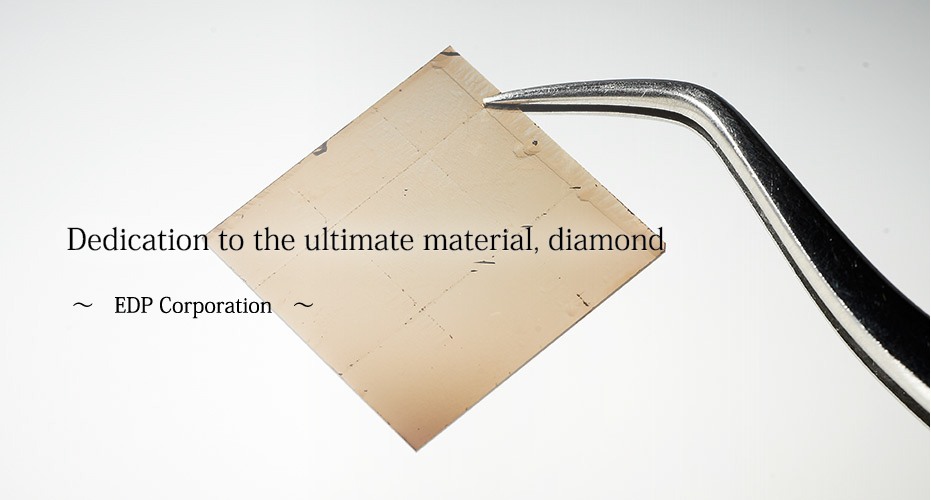
TECH Meets BUSINESS
In 2009, the long-time research dedicated to the study of diamond at AIST led to the establishment of a startup company named “EDP Corporation.” The company successfully launched its business in materials manufacturing, the development of which takes a long time, and the business was soon fully operational. What is the reason for this success?
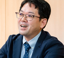
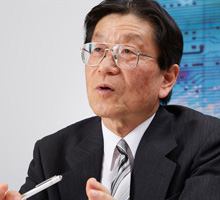
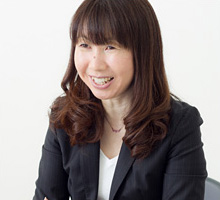
President of EDP Corporation. After being engaged in the research and development of diamond materials and their commercialization at a company, in 2003 he became Director of The Diamond Research Center, which was newly established at AIST. He founded a startup company based on the results of the development of production technology of “planar single crystals of diamond” at this center and, as the president of the company, he dedicates his time to technology development, while managing the company at the same time.

Diamond is the best material.
I heard that you were engaged in research at a materials manufacturer before you joined AIST. What kind of work did you do there?
I conducted research on materials and parts for electronics, and oversaw their product development and commercialization. I was engaged in the development of diamond materials, ranging from the development of long-term synthesis methods to the development of products.
-- What are the products of diamond itself?
Fujimori:They are tool products in a broad sense, and heat sinks, which are used to cool products. In addition, among unique products, there are tweeters, which are used to reproduce high-pitched sound for speakers. We made them of a thin hemispherical diamond with a thickness of no more than 30 micrometers. Diamond has excellent acoustical properties, and it is the best material for tweeters. Of course speaker sets in which they are used become extremely expensive, though.
-- After these experiences, you became Director of The Diamond Research Center at AIST. How did that happen?
Fujimori:Originally, it began when a national project dedicated to diamond research was started. It was a project in which many companies, universities, and other research institutes participated, and of course, AIST was also involved in the project. At that time, I received an offer from AIST and I became Director of the newly established research center. The project was specifically dedicated to devices, and the single crystals we were working on were required materials for those devices.
-- So, was the establishment of EDP an initiative of Division for Start-ups?
Fujimori:No, it was me who submitted this proposal to the Division for Start-ups. That was because I considered our research to already have advanced to a level at which commercialization was possible. I knew that AIST supported spinning off businesses at that time, so around 2008 we collaboratively began to prepare for starting our business. However, while we were discussing how to attract capital for production equipment, what has become known as “the Lehman Shock” occurred. Because of its impact, it was hard for us to source capital. I once almost thought that “we should give up.”

A possibility to scale up. This is why we started our business.
-- You decided to start a business during a recession. Was it because of your expectation and trust in that technology?
Fujimori:Yes, it was because we had diamond materials. Diamond is a very hard substance, and this is because the distance between neighboring carbon atoms that constitute diamond is short and the bond between those atoms is strong. This characteristic is linked to its properties of high thermal conductivity and high propagation of the speed of sound. The reason why diamond is used for expensive tweeters is because of these properties.
-- It attracts a great deal of attention as a semiconductor material, doesn’t it?
Fujimori:Please imagine the periodic table in chemistry. Carbon (C) is right above silicon (Si), which is a semiconductor material. These two elements are in the same group, and they have similar properties. Diamond is an insulator, which does not conduct electricity, and it is possible to turn this insulator into a semiconductor by adding impurities. Diamond has properties superior to those of silicon, such as thermal conductivity and high voltage endurance.
-- Other than its use as a semiconductor, are there any other possible uses?
Fujimori:In the first place, it is rare to find a substance with multiple properties that are more excellent than the properties of other substances. In most substances, a certain property may be excellent, but other properties are not. In contrast, diamond has many excellent properties such as hardness, thermal conductivity, insulation, and optical properties. Human beings have used only a few advantages of diamond. Increasing our usage thereof would enable us to consider ways in which to use it such that existing concepts could be changed.
-- Speaking of diamond, we can’t help imagining a gem, but many synthetic diamonds are produced for industrial use. How is diamond produced?
Fujimori:The present mainstream methods are a high-pressure, high-temperature synthesis method, and a chemical vapor deposition method. The former of these methods involves subjecting material carbon atoms to high pressures and high temperatures similar to the environment in which diamond is produced in nature. On the other hand, what we have chosen is the chemical vapor deposition method, and this is a method in which diamond is produced from a carbon-containing gas. We can produce diamond as though “frost were formed.”
-- What do you mean by as though frost were formed?
Fujimori:In winter, dew condensation is often seen on window glass. The principle is the same as that. Actually, this dew condensation “grow” from the surface of glass. Under certain conditions, moisture that cannot dissolve any further in air will "grow" from the glass surface as drop of water. We use this principle in a similar way, using a carbon-containing gas, such as methane gas. In the chemical vapor deposition method, the gas pressure is about 0.1 atmosphere, which is lower than atmospheric pressure, and the temperature is about 1000 degrees. Of course, there are various other conditions, but at this point, we can say that this method is easier than the high-pressure, high-temperature synthesis method.
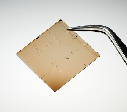
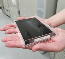
-- Then, you “peel off” the diamond that is produced, and you create a planar diamond, correct?
Fujimori:We use technology called “electrochemical etching,” which was developed at AIST. This method enables us to directly produce a planar diamond without going through granular diamonds. If we have a seed crystal, we can duplicate it to form a planar diamond with the same size.
-- Does this mean that you are only able to produce diamond with the same size as the seed crystal?
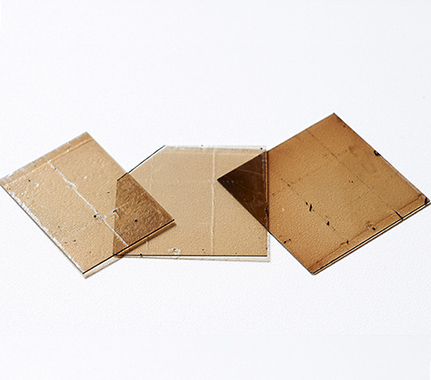
Fujimori:No, we can increase the size by positioning the produced planar diamonds vertically and horizontally and using them as a seed crystal. I remember that I recognized a promising business opportunity at this point. If we can produce a large single crystal, the range of application as material becomes large. For example, to use it as semiconductor wafers, the size needs to be about 2 inches. Right now, it is around 1 square inch, but we are conducting research and development so that we can produce larger ones, such as 2 and 3 square inches.
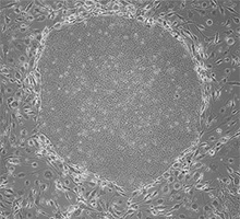
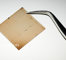
A large plate can be produced from multiple single crystal diamond plates.
Research and development are conducted to produce larger products.

Thinking of Japanese industry, I consider the manufacturing industry to be important after all.
-- I heard that commercialization was triggered when you realized a way to produce planar diamond in larger sizes.
Fujimori:Yes, the chemical vapor deposition method was already an established technique when we started our business. As you know, we thought that we could do well, when we saw a prospect to increase the size as a result of technological development at The Diamond Research Center in AIST. It was around the year 2007.
-- Could you tell me to which fields it will be applied in future?
Fujimori:For material, it is essential to collaborate with researchers of devices in which the material will eventually be used. For example, when a material is applied to semiconductor wafers, we will ask researchers to consider in which devices the material could be used if we were able to produce the material at a size of 2 square inches, also what would be possible if we were able to obtain an even larger size such as 3 and 4 square inches. Then, the next thing we will probably encounter is the problem of cost. Since the material will be sold as a product, manufacturers would like to manufacture it in a preferred price range.
-- Could you tell me about commercialized products?
Fujimori:Among the products we have launched since our company was founded, there are cutting tools. For example, when aluminum is chamfered, it is not possible to obtain a high-gloss surface without using cutting tools made of a sharp material such as a single crystal of diamond. Mostly, the sizes of diamond parts used in the blades of diamond cutters are small, but if a large planar blade is used, we can produce parts with accuracy that has been impossible to achieve so far. Actually, there are cases, for which the required accuracy is hard to achieve when a new product is made, and tools made of a single crystal of diamond are needed, and then, a large-sized single crystal produced in our company is used.
-- Demand for a material arises only if there is a request from the application side, doesn’t it?
Fujimori:That is also hard. Simply because we have the ability to produce a large diamond, it does not necessarily mean that a business opportunity exists. I think that the business only pays when an application is found for a product. It takes time until this occurs. We are asked whether we would be able to survive until then. Right now, there are various inquiries from manufacturers of tools and heat sinks, and from research institutes of diamond devices, and we are asked how we respond to them.
-- Lastly, tell me about the future prospects of EDP Corporation.
Fujimori:To launch and run a start-up company in the materials field, we need a lot of time, the cost of developing the product, and capital for purchasing equipment, but I think that what we need to do in Japan from now on is to focus on the manufacturing business, of course. This is what I have been thinking since I started this company. That is why I would like to continue doing this business in Japan. Although the size of the company may not be very large, I would like to make our company a major player in diamond manufacturers within several years in the future.
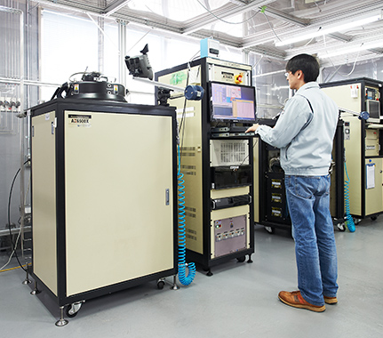
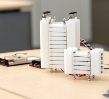
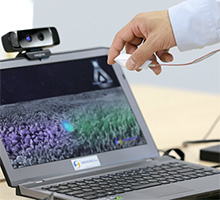
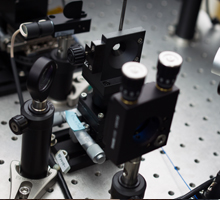
Synthesis equipment for the chemical vapor deposition method. Diamond is produced in this equipment.
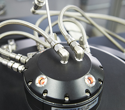
Diamond is produced as if “frost were formed,” by injecting gas into the device.
* The contents of this article are based on information as of January 10th, 2014.
![]()
株式会社イーディーピー
〒560-0085 大阪府豊中市上新田4-6-3
Mail. n.fujimori@d-edp.jp
https://www.d-edp.jp
*Application field
・精密切削工具、耐摩耗工具
・高出力/高温デバイス等の研究用基板(ウエハ)
・X線等の透過窓
・放射線/紫外線センサー
・ヒートシンク
EDP Corporation
4-6-3 Kami-Shinden, Toyonaka-shi, Osaka 560-0085, Japan
Mail. n.fujimori@d-edp.jp
https://www.d-edp.jp/en/
*Application field
- Precision cutting tools, wear resistant tools
- Substrates (wafers) for research of high-power/high-temperature devices
- Transmission windows for X-rays and so on
- Sensors for radiation/ultraviolet light
- Heat sinks
Research Institute for Earth Science Visualization Technology Co.,Ltd.
Visualizing the History of the Earth, and Creating a “Museum of the Future”!
- Precision 3D Modeling and Projection Mapping –

Mottainai Energy Co., Ltd.
Brightening the Future with Electricity Produced from Heat!
LEAG Solutions Corporation
New image measurement for the smart society!
- 3D position and attitude measurement using high-accuracy markers -

HikariPath Communications Co., Ltd.
Realtime 4K video eliminates distance using new optical communication technology!
Trimatiz Limited
Manipulating light to open up the future! Technology for measuring the unknown underwater world

Nanolux co. ltd.
Deliver Color Images in Darkness! Unique Technology Enabling Color Image only by Infrared Illumination
SteraVision Co.,Ltd.
Realizing an Eye that can See like a Human!
– Development of Optical Steering Device and New Standard Lidar -
ProteoBridge Corporation
Reproduce human on the palm !
-Development of the world's first human protein array-

Site Sensing Inc.
Expanding a New Business with Excellent Measurement Technologies for Tracking, 3D Modeling , and Face Recognition
Hmcomm Inc.
Controlling Voice to Open Up Next Generation Business!
- Commercializing AI and Voice Recognition Technology -
TOKIWA-Bio Inc.
Automatic Generation of iPS Cells!
- Contributing to Gene Therapy Worldwide -
HSP Technologies Inc.
Producing New Materials by Mixing Materials that do can not Mix!
MIRAISENS,Inc.
A feeling as if things were really there!
~ Digitization of physicality and bodily sensations ~
PicoTherm Corporation
Supporting information society by technology to measure thermophysical properties
EDP Co.
Dedication to the ultimate material, diamond

Research and Innovation Promotion Headquarters
Innovation Center for Startups
Tsukuba Center1, 1-1-1, Umezono, Tsukuba, Ibaraki 305-8560, JAPAN
E-mail:dsu-koho-ml@aist.go.jp