We have been studying the fundamental technologies for quantum computing and the integrated device technologies for ultra-low power and high-speed device operation. We have also been studying simulation technology for designing innovative silicon devices. We operate “Communal Fabrication Line for Outstanding Modern Devices; COLOMODE” and fabricate the devices using COLOMODE.
Exploratory Silicon Device Research TeamKeywords
Semiconductor
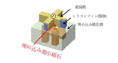
Silicon Qubit
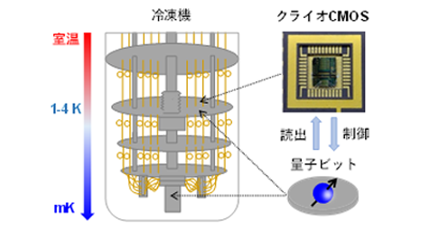
CryoCMOS
Tunnel transistor
Impulse TCAD
Exploratory Silicon Device Research TeamResearch Topic
Quantum computer has attracted much attention as next generation computer which enable us to solve various problems such as the optimization of traffic and logistics, the prediction of the material characteristics etc. Our team has been studying silicon quantum computers, which are one of the leading candidates for practical quantum computing hardware. Silicon-based quantum computers have the advantage of using mature semiconductor process technology, which has achieved integration of more than 1 billion transistors. We are developing the technology for silicon qubit fabrication using COLOMODE. We are also developing the quantum device simulator for designing the qubit and proposing novel structures for qubit integration.
2. Cryo-CMOS
For realizing large-scale integration of quantum computers that operate in dilution refrigerator, we need to place the semiconductor circuits specialized for qubit control and readout in the refrigerator. The technology for manufacturing the semiconductor circuits for such cryogenic operation is called "Cryo-CMOS" technology. Our team is conducting research and development of cryo-CMOS technology from the viewpoint of both circuit design and device physics.
3. Steep switching devices
Recently, MOSFETs are reaching their limits in terms of high performance and low power consumption by miniaturization. Therefore, the development of "steep switching devices," which can switch from off to on with a smaller input voltage than MOSFETs by utilizing a novel operating principle, has been attracting attention. Our team has been studying tunnel field effect transistor (TFET), which is a representative candidate for steep switching devices. We are challenging to develop high-performance TFETs for practical use by correctly controlling the material characteristics in nanometer-order semiconductor devices.
Exploratory Silicon Device Research TeamFacility
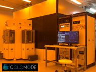
COLOMODE
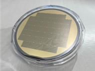
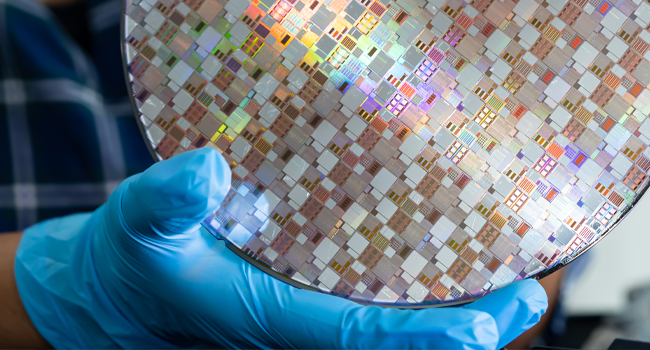
COLOMODE (Communal Fabrication Line for Outstanding Modern Devices; COLOMODE) is primarily operated by our team. COLOMODE is a facility having the equipment required for semiconductor device fabrication such as deposition,etching and lithography etc., and thus, we can complete the device fabrication in the COLOMODE. All COLOMODE's equipment are compatible with 4-inch wafers, and the variation within and between 4-inch wafers is extremely small, enabling stable processes to be carried out one after another at high speed. As for lithography, notable feature of our system is that we use both maskless exposure systems and electron beam lithography systems. Digital data of layouts drawn by researchers can be directly input without making masks (pattern base plates), and large patterns (um order or larger) to small patterns (30 nm to um order) can be handled.
Research and development of silicon qubits and cryo-CMOS requires a cryogenic measurement environment. Our team manages and operates one of the best measurement facilities in Japan dedicated to cryogenic evaluation of semiconductor devices. In addition to a dilution refrigerator capable of cooling to an ultra-low measurement temperature of 15 millikelvin, we manage a total of five refrigeration units. Moreover, a total of five semiconductor device parameter analyzers and noise measurement devices have been installed as measurement equipment.
Exterior view of low temperature measurement room
Dilution refrigerator
Refrigerant-free refrigerator
The 300 mm wafer cryogenic auto-prober enables high-speed and high-volume measurements at cryogenic temperatures, which have been difficult to achieve so far. The installation of this equipment is first in Asia, and the third in the world following Intel Corporation of the U.S. and the French Institute of Electronics and Information Technology (Leti).
Exploratory Silicon Device Research TeamJoint research