CMOS Integration Research TeamAbout
Technology in single-nanometer precision.

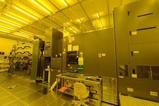
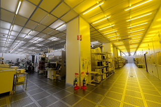
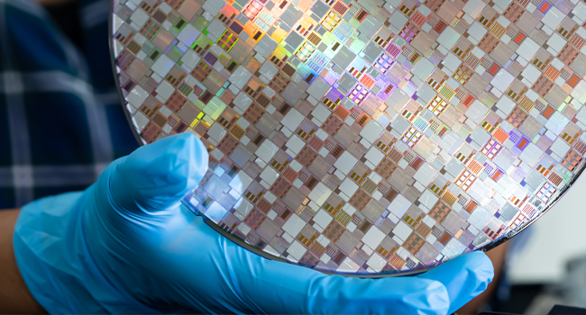
A semiconductor chip, commonly known as a Large-Scale Integrated (LSI) circuit, consists of complementary metal-oxide-semiconductor field-effect transistors (CMOS), comprising both positive-type and negative-type transistors. CMOS devices are continually miniaturized year by year. Presently, state-of-the-art LSI chips integrate billions of transistors, transforming their structure from a 2-dimensional planar type to 3-dimensional gate-all-around structures. Amid the era of the increasingly complex CMOS manufacturing processes described above, the CMOS Integration team is focused on creating groundbreaking technologies which are applicable to a few chip generations at Super Clean Room in AIST-WEST, Tsukuba.


