Super Clean Room(SCR)
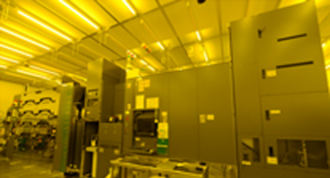
We have semiconductor processing equipment for 300mm wafers in a 3,000m2 Class 3 cleanroom. We can perform R&D using existing process menus, individual processes, and stand-alone processing.
SCR WebsiteCOLOMODE (Communal Fabrication Line for Outstanding Modern Devices)
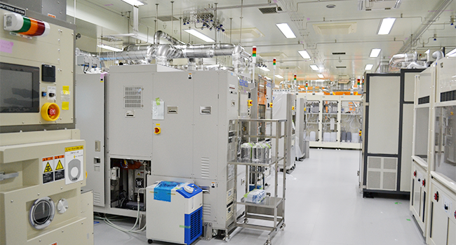
A cleanroom for prototype research and development of next-generation semiconductor electronic devices, with capabilities focused on the implementation of silicon semiconductor device processes using 4-inch wafers.
COLOMODE WebsiteIMPULSE TCAD (Semiconductor device simulator)
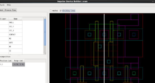
Impulse TCAD is a semiconductor device simulator originally developed by AIST to keep pace with future trends in semiconductor devices. It is equipped with automatic differentiation to facilitate the incorporation of physical models and parallel analysis to enable large-scale analysis.
More Details