Device Process Research Team
We are developing fundamental technologies related to materials, devices and fabrication processes used in semiconductor integrated circuits. From the creation of basic core technologies to the device demonstrations using state-of-the-art 300 mm equipment are consistently promoted.
Read MoreCMOS Integration Research Team

We contribute to the establishment of innovative technologies in the semiconductor industry, where CMOS manufacturing processes are evolving into greater complexity.
Read More300mm Processing Platform Research Team

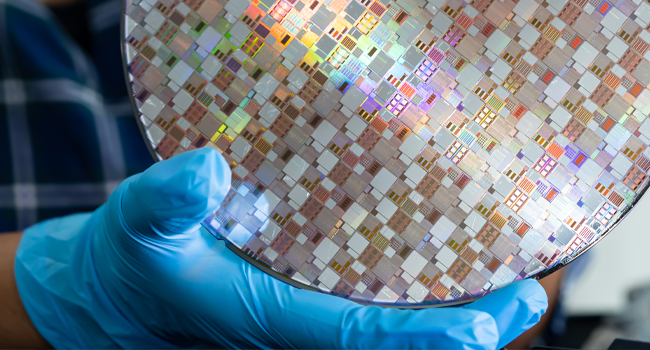
We provide R&D and fabrication services of semiconductors using 300mm silicon wafers at Super Clean Room (SCR) located in AIST Tsukuba West. In our leading-edge semiconductor R&D, the preparation of the open pilot line with the latest semiconductor process equipment in SCR is now ongoing.
Read MoreExtremely scaled CMOS materials Research Team

As a cutting-edge CMOS technology, we are actively advancing R&D with a focus on CMOS transistors, materials, processes, simulations, and TCAD for the 2 nm generation and beyond.
Read MoreExploratory Silicon Device Research Team

We have been studying the fundamental technologies for quantum computing, and the integrated device technologies for ultra-low power and high-speed device operation.
Read MoreIntegrated Circuit Design Research Team
In the cyber-physical system that society is rapidly becoming accustomed to, we aim to research and develop cutting-edge integrated circuit and system technology that will dramatically improve the energy efficiency of information processing, as well as to develop an integrated circuit design and development environment.
Read MoreDevice Simulation Research Team

We develop simulation technologies that can model semiconductor devices from their fabrication processes to their operational behavior. Using these tools, we aim to explore new device concepts, predict their performance, and analyze their behavior to support future design and development.
Read MoreSecure Integrated Circuit Research Team

We contribute to establishing secure information infrastructure through R&D of the secure design, manufacturing, and utilization of semiconductor integrated circuits.
Read More