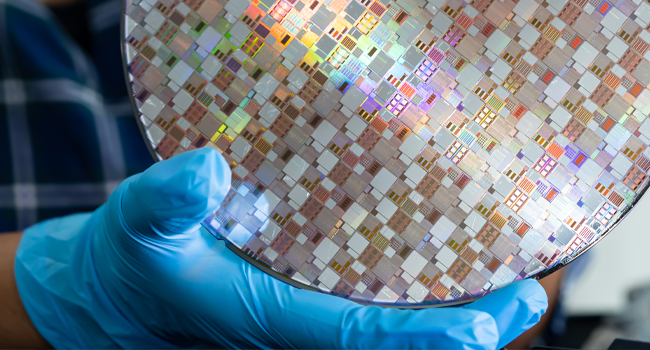
We are working on the research and development of cutting-edge devices such as nanosheet transistors used in semiconductor integrated circuits at the 2 nm node and beyond. With state-of-the-art 300 mm equipment, we are developing device fabrication processes to achieve higher performance, lower power consumption, and higher reliability. In addition, in collaboration with other teams, research on new material devices to overcome the limits of conventional Si devices are performed.
We are conducting research and development on Si nanosheet transistors, which will be introduced for the 2 nm generation and beyond, by utilizing the cutting-edge process equipment installed on our 300 mm line. Specifically, we will develop process technologies such as Si nanosheet channel formation by using Si/SiGe epitaxial growth technology, high impurity concentration low resistance source/drain formation, and high dielectric constant gate insulating film and metal gate electrode formation on nanosheet channels. In addition, we are concurrently proceeding with device demonstrations by integrating these elemental process technologies.
Looking ahead to the more advanced technology node beyond 2 nm, we are also conducting research on two-dimensional semiconductors and oxide semiconductors in collaboration with other teams, which are expected to become post-Si materials. Here, we are developing film deposition processes and device fabrication processes, while conducting research to deepen the device physics.