Our aim is to research and develop circuit technology that executes AI processing with high efficiency and low power consumption, organic transistor large-scale digital circuit technology, authentication systems using PUF, cryo-CMOS circuit technology for quantum computers, analog and digital integrated circuit technology for physical and chemical sensors, and to explore an LSI design and development environment using open source EDA.
Research on methods for determining the authenticity of semiconductor chips and building a root of trust
CAnalog mixed-signal IC design for MEMS sensor devices
Research and development of edge AI chips that can perform ultra-highly efficient AI processing
Realization of digital circuits using printed devices
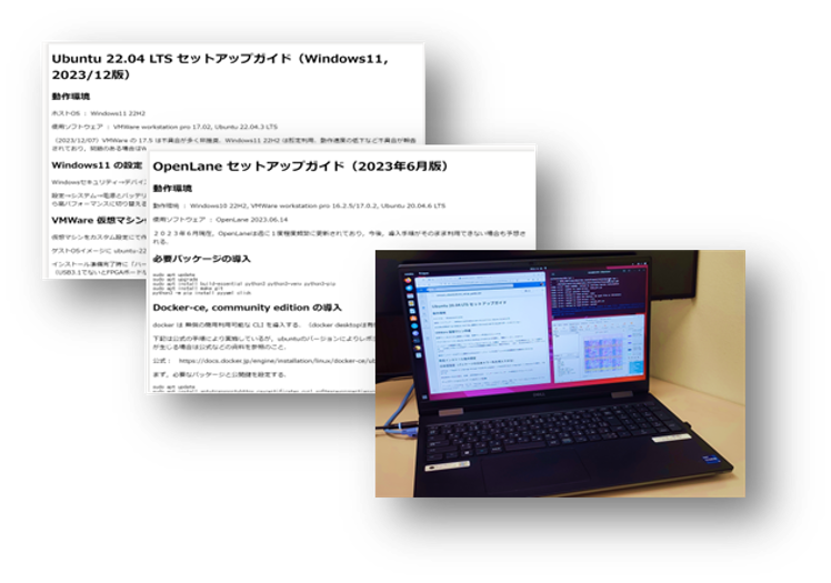
Exploring an LSI development environment using OpenSource EDA
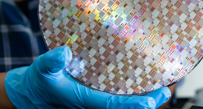
Semiconductors are used everywhere, from consumer electronics to industrial products and critical infrastructure. They are essential for a comfortable and convenient society. However, the proliferation of counterfeit semiconductor products and information leaks from IoT devices has been of great concern in recent years. For secure and safe IoT/CPS (Cyber-Physical Systems), it is crucial that semiconductor products are genuine and that data security is guaranteed. To realize secure and safe IoT/CPS, we are conducting research and development on Physically Unclonable Functions (PUFs). PUFs utilize the inherent “variability” in semiconductors to authenticate individual IC chips and generate cryptographic keys for data protection. This technology effectively prevents device replication and counterfeiting, and it can be implemented at a low cost.
Analog mixed-signal integrated circuits for MEMS sensors include various essential components such as low-noise amplifiers, AD converters, and digital circuits. In this study, after modeling sensor device as an equivalent circuit, its appropriate circuit architecture will be created to satisfy given specifications and/or target cost. We also adopt digitally-assisted techniques to enhance its performance and functionalities. This sensor circuit co-optimization scheme can be applicable to other devices such as actuators and energy harvesting as well.
AI (deep-learning) tasks are usually processed in data centers because of the huge amount of computation. However, it is expected that AI tasks are processed at user side, due to large power and latency in communication between users and data centers and security concerns. In user side (edge) devices, the power allowed for AI tasks is often limited. Therefore, circuits dedicated to process AI tasks efficiently, called “edge AI chips,” are required. We are conducting research and development of ultra-efficient AI chips.
Flexible printing devices have the characteristics of being inexpensive due to printing technology, flexible enough to be mounted on curved surfaces, and capable of mounting large-area sensors and circuit elements, and are expected to have the potential to greatly change the degree of freedom in the form of computers. I am. In order to realize a device in which many circuit elements are printed on a single flexible film, we are aiming to realize a digital circuit using a printed device.
OpenSource EDA has become a global trend, and cases of its use in Japan are gradually increasing. In this research, we are accumulating knowledge related to the development and use of a usage environment for the widespread use of OpenSource EDA/PDK in Japan.