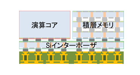
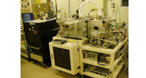
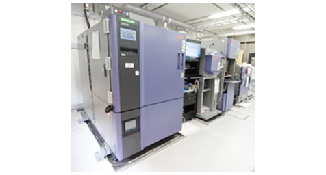
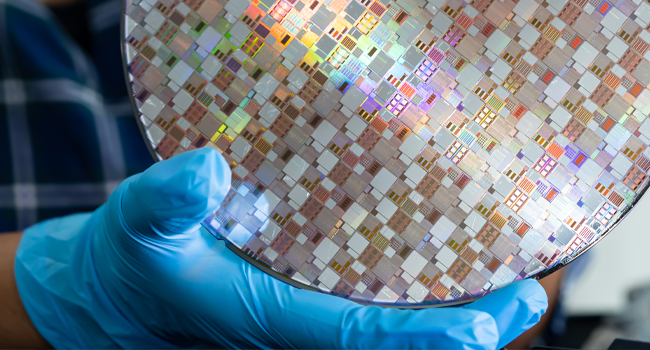
We are conducting research and development on building an integrated circuit design platform with a chiplet structure and increasing the scale of superconducting quantum computing systems by applying 3DIC technology. Manufacturing of through-Si via (TSV), narrow pitch bump formation, and direct bonding are also developed as our core technology. In addition to these fabrication techniques, we are also researching electrical and thermal analysis and electrical, evaluation and reliability.
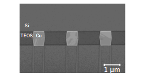
Planer interface pads are activated and bonded within vacuum condition. This technology arrows room temperature bonding of two materials.
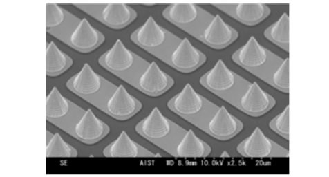
Our original technique to form cone-shaped bump enables extremely small and narrow pitch interconnect.
We investigate process technologies including interposer, bump, and integration to develop integration technology of chiplet.
We develop low temperature bonding technology to protect fragile qubits and direct bonding technology between superconductive materials.
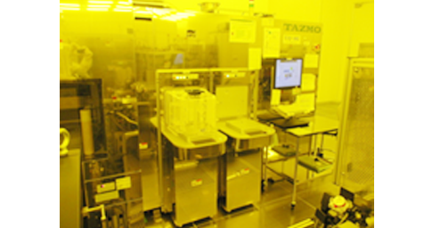
Thick metal pattern with TSV is buried onto a large area which was never used before. The buried metal provides drastic improvement of power integrity of 3DIC.
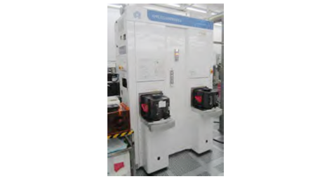
This machine forms TSV via-hole by accurate controlling etching gas.
It enables wafer-bonding in vacuum after precision wafer alignment.
bonding machine for chip to chip bonding, with various parameters including load and temperature while bonding.
Cone-shaped bump can be fabricated with self-formation, by spraying nanoparticles using carrier gas.
Thermal cycle test (TCT), high accelerated stress test (HAST), and constant temperature and humidity test chambers enables various types of reliability test.