
About Us
Research Institute for Advanced Electronics and Photonics (RIAEP) belongs to the
National Institute of Advanced Industrial Science and Technology(AIST)
which is one of the largest public research institutes in Japan.
RIAEP consists of 75 researchers from a wide range of research fields including theory, material, device, and system on electronics and photonics. Collaborating effectively with industry, academia, and government, we are conducting research and development on photoinduced processing technology and emerging electronics. We focus on two technology fields with 8 research groups as shown bellow.
RIAEP consists of 75 researchers from a wide range of research fields including theory, material, device, and system on electronics and photonics. Collaborating effectively with industry, academia, and government, we are conducting research and development on photoinduced processing technology and emerging electronics. We focus on two technology fields with 8 research groups as shown bellow.

1. Photoinduced Processing Technology
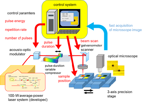
- For safe and secure society: pursuing ultra-short pulsed light and plasma
generation technologies and seeking its application to manufacturing processes,
life sciences and measurement technologies
Aiming at application to extreme measurement technology and next-generation processing technology, we promote the development of ultra-short pulsed lasers and application research such as pulsed light processing and plasma processing.
Through our research we hope to contribute to technological innovation in electronics, life and medical fields, and new materials development.
2. Emerging Electronics
- Creation of innovative electronics and photonics technology: from exploring
functional materials to developing energy-saving devices
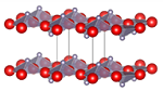
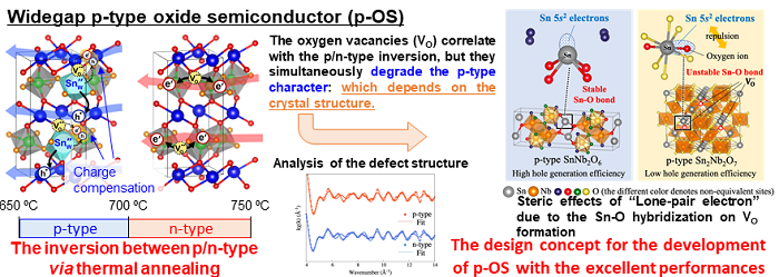
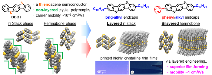
Our society is facing worsening environmental and energy situation on a global scale. Although the development of information and communications technology (ICT) has contributed to energy conservation, the major problem of ICT remains unsolved. Specifically, the energy consumption of ICT products needs to be reduced drastically by creating an entirely new type of devices beyond present technology. Toward that goal, we are carrying out research onemerging materials both from basic and applied points of view. The target materials are high-Tc superconductors, strongly-correlated oxides, and organic semiconductors, etc.
 Key themes for materials and devices:
-Ferroelectric resistive memories with low-voltage operation
-Mott field-effect transistors consisting of strongly-correlated electron systems
-Superconducting wires based on iron-based superconductors for persistent current magnets
-Novel superconductors exhibiting unprecedented functions
-Environmentally friendly lead-free piezoelectric materials
-Oxide electroluminescence (EL) devices with high luminous efficiency and environmental durability
-Photonic processing by pulsed light sources and its device application
-Carbon-nanotube based transparent conductive films
Our society is facing worsening environmental and energy situation on a global scale. Although the development of information and communications technology (ICT) has contributed to energy conservation, the major problem of ICT remains unsolved. Specifically, the energy consumption of ICT products needs to be reduced drastically by creating an entirely new type of devices beyond present technology. Toward that goal, we are carrying out research onemerging materials both from basic and applied points of view. The target materials are high-Tc superconductors, strongly-correlated oxides, and organic semiconductors, etc.
-Ferroelectric resistive memories with low-voltage operation
-Mott field-effect transistors consisting of strongly-correlated electron systems
-Superconducting wires based on iron-based superconductors for persistent current magnets
-Novel superconductors exhibiting unprecedented functions
-Environmentally friendly lead-free piezoelectric materials
-Oxide electroluminescence (EL) devices with high luminous efficiency and environmental durability
-Photonic processing by pulsed light sources and its device application
-Carbon-nanotube based transparent conductive films