
Correlated Electronics Group
Group Outline and Primary Goal
The target of our research and development is to trigger innovation in electronics by
establishing
fundamentals in advanced state-of-the-art electronic devices for information and communication technologies,
which will contribute to the creation of a low-carbon society.
Specifically, we develop technologies that control electric phase transitions where electric, magnetic, and optical properties change dramatically through external fields such as electric fields, magnetic fields, and lights, which is characteristic to strongly correlated electronic materials.
Specifically, we develop technologies that control electric phase transitions where electric, magnetic, and optical properties change dramatically through external fields such as electric fields, magnetic fields, and lights, which is characteristic to strongly correlated electronic materials.
Key Themes of Research
- Developments of state-of-the-art functional materials such as multiferroic materials with magnetic properties controlled by external voltage; colossal-magnetoresistance materials with a resistance change as large as several orders of magnitude; superconductors; thermoelectric materials with large figure of merit.
- Development of crystal growth technology of high-purity, low-defect, and large-diameter single crystals of β-Ga2O3 as a next-generation power semiconductor.
- Developments of prototypical electronic and neuromorphic devices such as Mott transistor utilizing a gate-controlled Mott transition (metal-insulator transition) of the strongly-correlated material; nonvolatile resistive random access memory (ReRAM) exploiting the switching of electric polarization in ferroelectric materials; their application to emerging computer technologies.
- Development of optical switch by a new mechanism combining silicon optical waveguide with strongly correlated material exhibiting a metal-insulator transition.
- Development of high-resolution magneto-optical microscope with time-resolved observation technique for
magnetic domain dynamics by the stroboscope method.
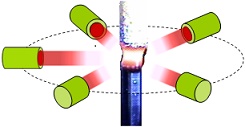
Schematic picture of originally developed crystal growth technique by the floating zone method using laser diodes as a heating source (LDFZ method)
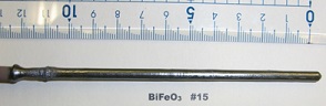
A large-sized single crystal of a room-temperature multiferroic material BiFeO3 using LDFZ method
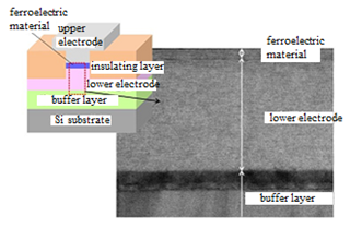
Schematic picture of ferroelectric resistance change memory device and scanning transmission electron microscope image of the cross section of the device
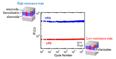
Characteristics of rewriting data in ferroelectric resistance change memory devices by applying voltage pulses (arrows indicate the direction of electric polarization of the ferroelectric tunnel barrier layer)
Our Technologies
- High-quality single-crystal growth of metal oxides utilizing the laser-diode-heated floating-zone (LDFZ) furnace
- Fabrication of atomically flat heterojunctions and superlattices of strongly-correlated materials by pulsed laser deposition
- Device fabrication process for new functional materials such as metal oxides
- High resolution magneto-optical microscope