
Innovative Plasma Processing Group
Group Outline and Primary Goal
Our goals are to develop innovative energy-saving and low-environmental-load
electronics devices through advanced control of plasma process technology, and to share the results with
society. In this way, we contribute to the realization of a safe and secure super-aging society.
Key Themes of Research
1. R & D of novel processing technologies such as nitride materials, carbon materials, surface treatment
and passivation, etc.
1-1. Production of low- temperature high-density nitrogen radicals under moderate pressure condition
* Development of high-efficiency green and red LED elements
* Development of nitrogen passivation technology for semiconductors
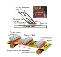
1-2. Large area and high-throughput surface treatment by damage less low- temperature plasma processes at the atmospheric pressure (see. Fig.1)
1-3. Production of carbon materials
* Growth of high-quality graphene film at low-temperature
(High performance heat dissipation materials for highly integrated and thin-film electronic devices)
* Atomic carbon source using long-duration discharge, etc.
1-4. Development of high-power green laser
* Modeling using numerical simulation
(Defect control of oxide optical materials induced by a laser)
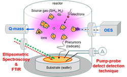
1-5 Semiconductor plasma diagnostics and defect control technology (see. Fig.2)
* Real time in-situ detection technique of semiconductor defects
* Improvement of the semiconductor material propertiess via defect reduction
* New and unique applications for silicon-based thin film materials
2. Research and Development of life science;
* Translational research for minimally invasive plasma hemostatic devices for surgical operations (see Fig.3)
* International standardization research (IEC / TC 62-SC 62D–MT34)
* Development of processing technology for pharmaceutical preparation by low-temperature highly reactive plasma
* Development of near-infrared imaging sensors
* Processing of low-toxicity boron preparation for neutron capture therapy
3. Basic Research
* Research on charge control of materials using plasma technology
* Development of ultra-miniature plasma thruster for ultra-microsatellite
1-1. Production of low- temperature high-density nitrogen radicals under moderate pressure condition
* Development of high-efficiency green and red LED elements
* Development of nitrogen passivation technology for semiconductors
1-2. Large area and high-throughput surface treatment by damage less low- temperature plasma processes at the atmospheric pressure (see. Fig.1)
1-3. Production of carbon materials
* Growth of high-quality graphene film at low-temperature
(High performance heat dissipation materials for highly integrated and thin-film electronic devices)
* Atomic carbon source using long-duration discharge, etc.
1-4. Development of high-power green laser
* Modeling using numerical simulation
(Defect control of oxide optical materials induced by a laser)
1-5 Semiconductor plasma diagnostics and defect control technology (see. Fig.2)
* Real time in-situ detection technique of semiconductor defects
* Improvement of the semiconductor material propertiess via defect reduction
* New and unique applications for silicon-based thin film materials
2. Research and Development of life science;
* Translational research for minimally invasive plasma hemostatic devices for surgical operations (see Fig.3)
* International standardization research (IEC / TC 62-SC 62D–MT34)
* Development of processing technology for pharmaceutical preparation by low-temperature highly reactive plasma
* Development of near-infrared imaging sensors
* Processing of low-toxicity boron preparation for neutron capture therapy
3. Basic Research
* Research on charge control of materials using plasma technology
* Development of ultra-miniature plasma thruster for ultra-microsatellite
Fig.1 Next-generation microstrip line type of microwave process tools capable of low-temperature atmospheric pressure plasma treatment using various gases at high speed, mass processing, low cost, low power, compact size, and long life.
Fig.2 Semiconductor plasma diagnostics
Plasma diagnostics, using electricidal probe, emission spectroscopy, mass spectrometry, absorption
spectroscopy, and other techniques. Material characterization, using spectroscopic ellipsometry, FTIR,
and pump-probe defect detection techniques.
Fig.3 Minimally invasive plasma hemostasis equipment for open surgery
Our Technologies and Equipment
- Plasma generation technologies under low-, moderate-, and atmospheric-pressure regions, solid element-derived plasma production technologies, ion beam technologies, numerical simulation technologies, and diagnostic technologies
- Plasma equipment for low-, moderate-, and atmospheric-pressure regions, Raman microscopy system, low-resistance meter for thin-film, surface energy measurement equipment, spin coating, plasma spectrometer (UV, visible, and near-infrared regions),infrared camera, ion beam equipment, YAG laser, high-voltage power supply, etc.
- Plasma CVD (with semiconductor gas equipment), inorganic draft chamber, QSSPC (carrier lifetime measurement), sub-gap optical absorption spectroscopy, pump-probe defect detection equipment