
Compound Semiconductor Device Group
Group Outline and Primary Goal
We promote the development of innovative photonic and electronic devices composed of compound and organic
semiconductors that exhibit new physical and quantum effects by integrating advanced crystal growth
technologies, nano- /micro-level microfabrication process technologies, high-performance circuit design
technologies and leading evaluation technologies.
Key Themes of Research
1) Development of highly reliable quantum dot yellow semiconductor lasers
2) Development of high-efficiency and high-directional
micro-LED
3) Compact and high power (quick charging) wireless power transfer (WPT) technology using GaN electronic device
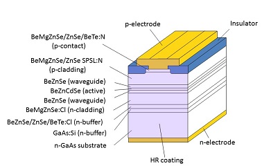
Schematic of a semiconductor laser
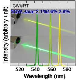
Photograph and spectra showing the continuous wave operation at room temperature of a BeZnCdSe quantum-well semiconductor laser
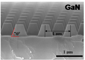
SEM image of the small truncated cones fabricated on the surface of a GaN blue LED
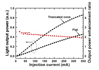
Comparison of the light output intensity of a truncated-cone type LED with
that of a flat-surface device.
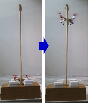
3) Compact and high power (quick charging) wireless power transfer (WPT) technology using GaN electronic device
Demonstration of GaN-WPT using a drone
Our Technologies and Equipment
- MBE crystal growth technology of group III-V and II-VI compound semiconductors
- MOCVD crystal growth technology of group III-V compound semiconductors
- Fabrication and characterization technology of semiconductor lasers, light-emitting diodes, etc.
- Fabrication and characterization technology of organic semiconductor thin films
- Physical property characterization technology, such as delayed luminescence, photoluminescence, and temporal- /spatial-resolved photoluminescence
- High-speed WPT technology and high-performance compact power-conversion circuit
- Analysis technology for abnormality portent in equipment