

グループ概要
化合物半導体デバイスグループ
研究目標
高度な結晶成長技術、ナノ・マイクロレベルの微細加工プロセス技術、高性能回路設計技術、先端計測・評価技術等を融合して、新たな物理・量子効果を発現させる革新的な化合物半導体・有機半導体電子光デバイス開発を推進します。
研究課題
1) 高信頼量子ドット型黄色半導体レーザの開発
2) 電流注入型高指向性マイクロLEDの開発
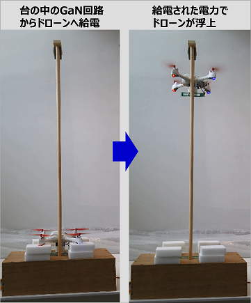
 3) GaN電子デバイスを用いた小型・大電力(急速充電)ワイヤレス給電技術
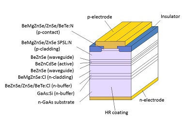
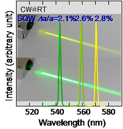
BeZnCdSe量子井戸半導体レーザーの素子構造と室温連続発振特性
2) 電流注入型高指向性マイクロLEDの開発
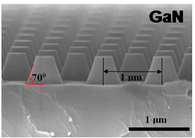
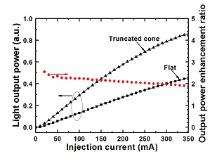
GaN青色LEDの表面に形成された微小円錐台のSEM写真
微小円錐台のある試料と平坦表面試料との発光強度の比較
GaNワイヤレス給電によるドローンTouch&Go
保有技術
- III-V族、II-VI族化合物半導体のMBE結晶成長技術
- III-V族化合物半導体のMOCVD結晶成長技術
- 半導体レーザー、発光ダイオード等の作製・評価技術
- 有機半導体薄膜の作製・評価技術
- 遅延発光、時間・空間分解フォトルミネセンスなどの材料物性評価技術
- 高速ワイヤレス給電技術、高性能小型電力変換回路
- 設備異常予兆分析技術
主要特許・論文
【2024】
- H. Yamada et al., "Metal-organic Chemical Vapor Deposition of n-AlGaN Grown on Strain-Relaxed Distributed Bragg Reflector Buffer Layers", Phys. Status Solidi B, 2300558 (2024).
- T. Gotow et al., "Characterization of InN Grown Directly on Sapphire Substrate Using Plasma-Enhanced Metal Organic Chemical Vapor Deposition", CRYSTAL RESEARCH AND TECHNOLOGY, 2400124 (2024).
- M. Nagase et al., " Nonvolatile memory operations using intersubband transitions in GaN/AlN resonant tunneling diodes grown on Si(111) substrates", JOURNAL OF APPLIED PHYSICS, 135, 145704 (2024).
- S. Gozu et al., "Size Control and PL Characteristics of InSb Quantum Dots on GaSb Substrates Grown by Molecular Beam Epitaxy", Phys. Status Solidi A, 2300659 (2024).
- 鍛冶 他、「センサ装置、信号解析システムおよび信号解析方法」、登録第7281763(2023/05/18).
- M.Nagase et al., “Enhancement of nonvolatile memory characteristics caused by GaN/AlN resonant tunneling diodes”, Semiconductor Science and Technology 38, 045011 (2023).
- S. Miura et al., “Analysis of terahertz double dielectric structure patch antenna using nitride semiconductors”, Electronics and Communications in Japan 106, e12390 (2023).
- Gozu et al., “Photoluminescence of GaAsSb/AlAsSb superlattices for investigating band structure”, Journal of Luminescence 263, 119955 (2023).
- T. Ide, "Recent researches of GaN-based materials and devices in NU-AIST", 2023 IEEE International Meeting for Future of Electron Devices, Kansai (IMFEDK), 1.
- T.Jinjyo et al., "Observation of Size-Dependent Optical Properties Based on Surface and Quantum Effects in Nanocrystals of 5,5'-Bis(4-Biphenylyl)-2,2'-Bithiophene", Adv.Photonics Res. 2100323 (2022).
- T.Matsuo et al., “Optically pumped lasing in a single crystal cavity of thiophene/phenylene co-oligomers grown via improved crystal growth methods in solution”, Appl.Phys.Express 15, 051002 (2022).
- N.Kumagai et al., “Comprehensive characterization of low-damaged GaN surface exposed to NH3 plasma toward plasma-induced metalorganic chemical vapor deposition”, Appl.Surf.Sci. 591, 153150 (2022).
- S.Gozu, “Photoluminescence of an InSb layer on a germanium substrate”, Semiconductor Science and Technology 37, 065002 (2022).
- H.Sakakita et al., “Ammonia-free epitaxy of single-crystal InN using a plasma-integrated gas-injection module”, Appl.Mat.Today 27, 101489 (2022).
- 鍛冶 他、「システムバランス変動予兆…」, 特願2022-061434 (2022).
- T.Ide et al., “Dynamic characteristics and device degradation of GaN-based vertical-cavity surface-emitting laser with an AlInN/GaN distributed Bragg reflector”, Jpn.J.Appl.Phys. 60,SBBE01 (2021).
- H.Mizuno et al., “Distributed feedback laser with methylammonium lead bromide embedded in channel-type waveguides”, Jpn.J.Appl.Phys. 60, SBBH11 (2021).
- N.Kokubo et al., “Analysis of Dislocations Line Tilts in GaN Single Crystal by Raman Spectroscopy”, Jpn.J.Appl.Phys. 60, SAAD03 (2021).
- H.Yamada et al., Appl.Phys.Lett. 118, 112101 (2021).
- R.Iida et al., “Large aperture GaN-based vertical-cavity surface-emitting lasers with nano-height cylindrical waveguide formed by BCl3 dry etching”, Appl.Phys.Express 14,012003 (2021).
- H.Mizuno et al., "Impact of material parameters on strong exciton–photon coupling states formed in microcrystal resonators of p- and n-type thiophene/phenylene co-oligomers", J.Mater.Chem.C 9, 11189 (2021).
- N.Kurahashi et al., "Micro-ring laser with CH3NH3PbBr3/PEO composite coated inside microcapillary", AIP Advances 11, 095301 (2021).
- S.Ando et al., “Impact of gate electrode formation process on Al2O3/GaN interface properties and channel mobility”, Appl.Phys.Express 14, 081001 (2021).
- Y.Ishikawa et al., “Generation of dislocations from scratches on GaN formed during wafer fabrication and dislocation reactions during homoepitaxial growth”, Jpn. J. Appl. Phys. 60, 115501 (2021).
- N.H.Trung et al., “Fabrication and analysis of InAlN/GaN metal–insulator–semiconductor high-electron-mobility transistors based on AlN/GaN superlattice channel”, Appl.Phys.Lett.119, 143503 (2021).
- Y.Miyake et al., “Synthesis of carbon nitride oligomer as a precursor of melon with improved fluorescence quantum yield”, Materials Advances 2, 6083 (2021).
- N.Kumagai et al., “Mobility and activation energy of lateral photocurrent of InAs quantum dot layers with ultra-fast carrier relaxation”, Physica E: Low-dimensional Systems and Nanostructures 126, 114478 (2021).
- M. Nagase et al., “Growth and Characterization of GaN-based Resonant Tunneling Diodes for High-Performance Nonvolatile Memory”, Physica Status Solidi A 218, 202000495 (2021).
- 井手、「ノイズ抑制回路、回路基板、及び電子機器」,110100310(台湾)、(2021).
- 秋本、「活性層・半導体発光素子及び活性層の製造方法」、特願2021-127353 (2021).
- 王 他、「窒素化合物の製造方法及び製造装置」、特願2021-166589 (2021).
- 山田、「化合物半導体基板」,特願2021—212419 (2021).
- 井手 他、「導線・コイル・トランス」,特願2021-073950 (2021).
- T.Ide et al., “Reduction of radiated emission from resonance coil in GaN wireless power transmission circuit by using Nd-Fe-N magnetic material”, AIP Advances 10,025121 (2020).
- M.Tsutsui et al., “A New DC Electric Field Sensor and Direct Measurements of Ionosphere Sq Electric Fields”, IEEJ Transactions on Electrical and Electronic Engineering, 15-9,1271 (2020).
- S.Dokiya et al., “Organic light-emitting diodes with a PIN structure of only thiophene/phenylene co-oligomer derivatives”, Jpn.J.Appl.Phys. 59, 41004 (2020).
- K.Iwai et al., Single-Crystalline Optical Microcavities from Luminescent Dendrimers”, ANGEWANDTE CHEMIE-INTERNATIONAL EDITION 59, 12674 (2020).
- T.Matsuo et al., “Synthesis and characterization of methoxy- or cyano-substituted thiophene/phenylene co-oligomers for lasing application”, RSC Advances10, 24057 (2020).
- H. Yamada et al., “Comparative study of boron precursors for CVD-grown h-BN thin films”, Phys. Status Solidi A, 2000241 (2020).
- P. Potisat et al., “Fabrication by vaporized film deposition and in situ FET measurements of polycrystalline thiophene/phenylene co-oligomer films”, Jpn.J.Appl.Phys. 59, SDDA17 (2020).
- R.Akimoto,” A comparative study of the operational characteristics of CdSe quantum dots and BeZnCdSe quantum well laser diodes”, J.Appl.Phys. 127,013101 (2020).
- J.Pan et al., “Double-Layer Cross-Coupled Silicon Nitride Multi-Ring Resonator Systems”, IEEE Photonics Technology Letters 32-5, 227 (2020).
- K.Mizuno et al., “Fabrication and characterization of vertical microcavities containing a submicron particle film of 5,5’-di(4-biphenylyl)-2,2’-bithiophene”, Jpn.J.Appl.Phys. 59, SDDA14 (2020).
- N.Kurahashi et al., “Whispering Gallery Mode Lasing from CH3NH3PbBr3/PEO Composites Grown in a Microcapillary”, Journal of Physical Chemistry C 124, 3242 (2020).
- Y.Hara et al., “A polymer film with ultra-broadband optical gain characteristics”, Appl.Phys.Lett. 116, 063301 (2020).
- M.Nagase et al., “Growth and Characterization of GaN-based Resonant Tunneling Diodes for High-Performance Nonvolatile Memory”, Physica Status Solidi A-Applications and Materials Science 2000495 (2020).
- 井手 他、「同期整流回路、電源装置、及び電子機器」,特願2020-000496 (2020).
- 井手、「ノイズ抑制回路、回路基板、及び電子機器」,特願2020-004268 (2020).
- 野村 他、「静電容量型センサ」, 特6775800 (2020).
- 井手 他、「ノイズ抑制回路、回路基板、及び電子機器」,特願2020-192733 (2020).
- 井手、「ノイズ抑制回路、回路基板、及び電子機器」, PCT/JP2020/044991(WIPO)(2020).
- 井手 他、「同期整流回路、電源装置、及び電子機器」, PCT/JP2020/047592(WIPO)(2020).
- T.Ide et al., “NdxFe1-xNy Magnetic Core Application for Resonance Coil of 13.56 MHz GaN Wireless Power Transmission”, IEEE Transactions on Magnetics 2801605 (2019).
- T.Kamei et al., “Research Toward Heterogeneously Integrated InGaN Laser on Silicon”, Physica Status Solidi A 1900770 (2019).
- M.Nagase et al., “Switching characteristics of nonvolatile memory using GaN/AlN resonant tunneling diodes”, Jpn.J.Appl.Phys. 58, 091001 (2019).
- S.Zhai et al., “Dual-Layer Cross-Coupled Tunable Resonator System in a Three-Dimensional Si3N4 Photonic Integration Platform”, J.Lightwave Tech. 37-13,3298 (2019).
- F.Sasaki et al., “Electroluminescence from double heterostructures of perovskite semiconductors and thiophene/phenylene co-oligomers”, Jpn.J.Appl.Phys. 59, SDDC01 (2019).
- H.Yanagi et al., “Cooperative Behaviors in Amplified Emission from Single Microcrystals of Thiophene/Phenylene Co-Oligomers toward Organic Polariton Laser”, Advanced Optical Materials 7-17, 1900136 (2019).
- S.Dokiya et al., “Strong exciton-photon coupling in organic microcavity electroluminescence devices with thiophene/phenylene co-oligomer derivatives”, Applied Physics Express 12, 111002 (2019).
- T.Akasawa et al., “Fabrication of low-dimensional microstructures with distyrylbenzene derivatives”, Jpn.J.Appl.Phys. 59, SDDA07 (2019).
- T.Matsuo et al., “Indication of cooperative light amplification in 5,5”-bis(4-biphenylyl)-2,2’:5,2”-terthiophene single crystals at room temperature”, Jpn.J.Appl.Phys. 59, SDDB02 (2019).
- M.Era et.al., “Squeezed-Out Technique to Prepare High-Quality PbBr-Based Layered Perovskite Langmuir-Blodgett Films Applicable to Cavity Polariton Devices”, Langmuir 37, 12224 (2019).
- H.Tachibana et al., “Highly concentrated dispersion of methyl-terminated germanane by liquid exfoliation”, Jpn.J.Appl.Phys. 58, 105002 (2019).
- H.Tachibana et al., “Liquid exfoliation of ethyl-terminated layered germanane”, Jpn.J.Appl.Phys. 58, SIIB21 (2019).
- H.Tachibana et al., “Hole transport dithiophene-benzene copolymer for electroluminescence devices”, Jpn.J.Appl.Phys. 59, SCCA01 (2019).
- X.Sun et al., “Silicon nitride based polarization-independent 4 x 4 optical matrix switch”, OPTICS AND LASER TECHNOLOGY 119, 105641 (2019).
- H.Yamada et al., “Reduction in residual impurities in semi-polar (3 0 (3)over-bar (1)over-bar) and (2 0
(2)over-bar (1)over-bar) GaN grown by metalorganic vapor phase epitaxy”, J.Cryst.Growth 512,119
(2019).
- H.Yamada et al., “Chemical Vapor Deposition Growth of BN Thin Films using B2H6 and NH3”, PHYSICA STATUS SOLIDI B-BASIC SOLID STATE PHYSICS,1900318 (2019).
- H.Yamada et al., “Growth Temperature Effects of Chemical Vapor Deposition-Grown Boron Nitride Layer Using B2H6 and NH3”, PHYSICA STATUS SOLIDI B-BASIC SOLID STATE PHYSICS 1900521 (2019).
- F.Sasaki et al., “Optically pumped lasing of cyano-substituted thiophene/phenylene co-oligomer microcrystals fabricated by the slide boat method“, Jpn.J.Appl.Phys. 58-SB, SBBG05 (2019).
- N.Kumagai et al., “Fabrication of submicron active-region-buried GaN hexagonal frustum structures by selective area growth for directional micro-LEDs“, J.Crystal Growth 507, 437 (2019).
- N.Kumagai et al., “Effects of N2 and NH3 plasma exposure on the surface topography of p-GaN under quasi-atmospheric pressure“, Surfaces and Interfaces 14, 92 (2019).
- 中西 他、「半導体デバイス測定方法、半導体デバイス測定装置、およびプログラム」,特願2019-148022 (2019).
- 永瀬 他、「共鳴トンネルダイオード素子」,特6529051 (2019).
- R.Akimoto et al., “Vertically Coupled Suspended Silicon Nitride Microdisk Based Optical Sensor”, IEEE Photonics Technology Letters 30, 1507 (2018).
- S.Zhai et al., “Vertically integrated waveguide self-coupled resonator based tunable optical filter”, Optics Letters 43, 3766 (2018).
- Y.Higase et al., “High-gain and wide-band optical amplifications induced by a coupled excited state of organic dye molecules co-doped in polymer waveguide“, Optics Letters 43, 1714 (2018).
- V.C.Nguyen et al., “Single-crystal perovskite CH3NH3PbBr3 prepared by cast capping method for light-emitting diodes”, Jpn.J.Appl.Phys. 57, 04FL10 (2018).
- K.Bando et al., “Self‐Assembled Organic Crystalline Microring Cavities with High Q‐Factors”, Chem.Nano Mater. 4 936 (2018).
- D.Okada et al., “π-Electronic Co-crystal Microcavities with Selective Vibronic-Mode Light Amplification: Toward Forster Resonance Energy Transfer Lasing”, Nano Letters 18, 4396 (2018).
- X.Wang et al., “High‐Efficiency, High‐Power AlGaInP Thin‐Film LEDs with Micron‐Sized Truncated Cones as Light‐Extraction Structures”, Phys.Status Solidi A, 1700562 (2018).
- M.Nagase et al., “Stabilization of Nonvolatile Memory Operation Using GaN/AlN Resonant Tunneling Diodes by Reduction in Structural Inhomogeneity”, Jpn.J.Appl.Phys. 57, 070310 (2018).
- N.Kurahashi et al., “Whispering gallery mode lasing in lead halide perovskite crystals grown in microcapillary”, Appl.Phys.Lett. 113, 011107 (2018).
- S.Gozu et al., “Highly strained InAlP/InGaAs- based coupled double quantum wells on InP substrates”, Jpn.J.Appl.Phys. 57, 055501 (2018).
- X.Shen et al., “Impact of strain state on the ultrathin AlN/GaN superlattice growth on Si(110) substrates by metalorganic chemical vapor deposition”, Jpn.J.Appl.Phys. 57, 010306 (2018).
- R.Akimoto, “Recombination-Enhanced Effect in Green/Yellow Luminescence from BeZnCdSe Quantum Wells Grown by Molecular Beam Epitaxy”, J.Electron.Mater. (2018), https://doi.org/10.1007/s11664-018-6090-3.
- V-C.Nguyen et al., “Single-crystal perovskite CH3NH3PbBr3 prepared by cast capping method for light-emitting diodes”, Jpn.J.Appl.Phys. 57, 04FL10 (2018).
- 鍛冶 他、「電磁波抑制装置と電磁波抑制方法」、特願2018-114550 (2018).
- 2020 JEM Best Paper Award, 秋本良一, Journal of Electronic Materials (JEM), August 2018
- POSTER AWARD, 井手利英, 第80回応用物理学会秋季学術講演会, 「GaN-WPTにおけるNd-Fe-N付コイルによる放射電磁界の抑制」
- Top Downloaded Paper Award, 亀井利浩, Physica Status Solidi A, 1900770 (2019).
- 「窒化物半導体薄膜結晶を作製するための新手法を開発~窒素プラズマを供給して世界最高品質を実現~」プレスリリース 2022/4/27 (王・熊谷・山田 他).