Oxide Electronics and Materials Group


Group Outline and Primary Goal

Metal oxides and related ionic materials exhibit various functions such as semiconductivity, metallicity, dielectricity, and superconductivity, depending on the choice of crystal forms and composition.
We are working on the development of materials, the elucidation of the physical properties' mechanism, and the establishment of physical property control methods for metal oxides, that will lead to the creation of innovative functional devices.
In particular, we focus on the research project "Exploration of oxide and ionic semiconductor materials and development of elemental technologies for thin-film devices", aiming at realization of energy-saving and highly functional devices that exceed the limits of existing technology.


Key Themes of Research

  • Development of oxide semiconductors and analogous ionic materials, and their device realization
  • Development of basic technology for multilayer ceramic capacitors using ferroelectric nanoparticle materials
  • Development of lead-free piezoelectric ceramics and related devices
  • Subdividing a quantum as a new quantum technology


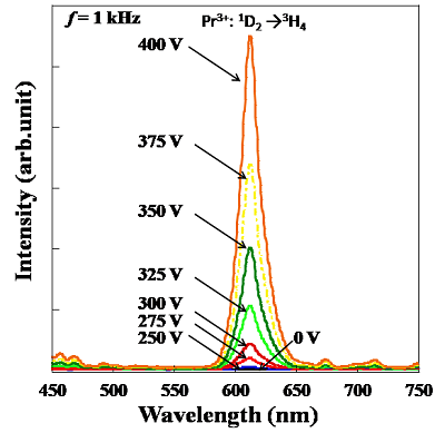
Electroluminescence using phosphor nanoparticle oxides. It eliminates the need for high-temperature heat treatment, therefore it has merits in terms of shortening processes, reducing manufacturing costs, and increasing the area.


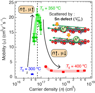
Low-temperature growth of p-type oxide semiconductor thin films using a high-power laser. Precise tailoring of both carrier density and mobility, which is dominated by the impurity scattering, is achieved.

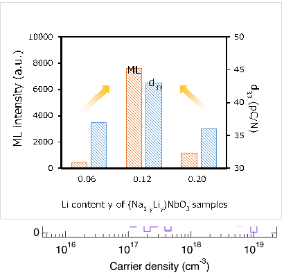
Development of Multi-piezo material that exhibits both piezoluminescence and piezoelectricity. Piezoluminescence is a form of mechanoluminescence (ML) during the elastic deformation. ML intensity increases with piezoelectric constant d33, indicating that piezoluminescence correlates closely with piezoelectricity in the Multi-piezo materials.


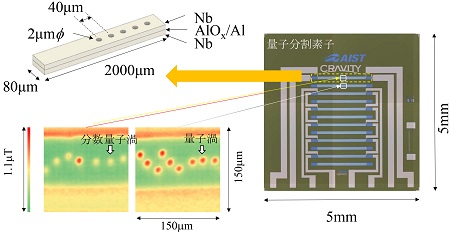
Successful generation of fractional flux quanta. The world's first successful direct observation of "fractional quantum vortex image as a phenomenon unique to two-component superconductivity". Zero electrical resistance, Meissner effect, and magnetic flux quantization are the three major superconducting properties governing from basic to application of superconductivity. However, fractional vortices deviate from those principles. We expect to open the way to quantum memory beyond the quantum limit. The generated mechanism of fractional flux quanta in the Josephson-coupled multicomponent superconductivity was discovered by AIST in 2001, and has been experimentally verified over the past 18 years. (Figure, upper left: Schematic diagram of the device; right, element subdividing a quantum; lower left, magnetic flux image of fractional vortex. Usual vortex image is also shown for comparison.)


Our Technologies

Variable temperature dielectric measurement prober, high temperature heating with concentrated infrared light, oxide solid phase reaction synthesis, oxide film formation through PVD process, X-ray diffractive structural analysis of thin film, design, fabrication and simulation technology for subdividing a quantum

Articles

  • R. Wang and H. Bando, PIEZOELECTRIC CERAMIC, AND PIEZOELECTRIC, DIELECTRIC OR PYROELECTRIC ELEMENT USING THE SAME, US8354038, 2013.
  • Y. Tanaka, A. Iyo et al., Method for controlling inter-component phase difference soliton and inter-component phase difference soliton circuit device, US 8902018, 2014.
  • Y. Tanaka, A. Iyo et al., Quantum Turing machine, US 7400282, 2008.
  • M. Minohara, N. Kikuchi, K. Tsukuda, Y. Dobashi, A. Samizo, K. Nishio, X. He, T. Katase, T. Kamiya, and Y. Aiura, “Effect of intentional chemical doping on crystallographic and electric properties of the pyrochlore Bi2Sn2O7”, Materials & Design 216, 110549 (2022).
  • H. Ishizu, H. Yamamori, S. Arisawa, K. Tokiwa, Y. Tanaka, “Phase shifter based on an ultrathin superconducting bilayer with a through-hole for a superconducting device”, Physica C 595, 1354029 (2022).
  • K. Ozawa, Y. Aiura, D. Wakabayasi, H. Tanaka, T. Kikuchi, A. Toyoshima, and K. Mase, “Beamline commissioning for microscopic measurements with ultraviolet and soft X-ray beam at the upgraded beamline BL-13B of the Photon Factory”, Journal of Synchrotron Radiation 29, 400-408 (2022).
  • M. Minohara, I. Hase, and Y. Aiura, “Characteristic Electronic Structure of SnO Film Showing High Hole Mobility”, J. Phys. Chem. Lett. 13, 1165-1171 (2022).
  • M. Itoh, Y. Hamasaki, H. Takashima, R. Yokoi, A. Taguchi, and H. Moriwake, “Chemical design of a new displacive-type ferroelectric”, Dalton Transactions 51, 2610 (2022).
  • M. Minohara, S. Asanuma, H. Asai, Y. Dobashi, A. Samizo, Y. Tezuka, K. Ozawa, K. Mase, I. Hase, N. Kikuchi, and Y. Aiura, “Elaboration of near-valence band defect states leading deterioration of ambipolar operation in SnO thin-film transistors”, Nano Select 3, 1012-1020. (2021).
  • Y. Tanaka, H. Yamamori, S. Arisawa, “Effective method of forming and detecting a fractional magnetic flux quantum”, Physica C: Superconductivity and its Applications 589, 1353932 (2021).
  • A. Samizo, M. Minohara, N. Kikuchi, K. K. Bando, Y. Aiura, K. Mibu, and K. Nishio, “Site-Selective Oxygen Vacancy Formation Derived from the Characteristic Crystal Structures of Sn-Nb Complex Oxides”, J. Phys. Chem. C 125, 17117-17124 (2021).
  • M. Minohara, Y. Dobashi, N. Kikuchi, A. Samizo, K. Tsukuda, K. Nishio, K. Mibu, H. Kumigashira, I. Hase, Y. Yoshida, and Y. Aiura, "Bipolar Semiconducting Properties in α-SnWO4 based on the Characteristic Defect Structure", Inorg. Chem.60, 8035-8041 (2021).
  • N.Oshime, K.Ueda, and H.Takashima, "Host Lattice-Excitation-Enhanced Photoluminescence in Eu3+-Doped LalnO3 Epitaxial Films", Cryst. Growth Des. 22, 2663(2021).
  • Y. Aiura, K. Ozawa, K. Mase, M. Minohara, and S. Suzuki, "Development of a high-precision XYZ translator and estimation of beam profile of the vacuum ultraviolet and soft X-ray undulator beamline BL-13B at the Photon Factory", J. Synchrotron Rad. 27, 923-933 (2020).
  • M. Minohara, A. Samizo, N. Kikuchi, K. K. Bando, Y. Yoshida, and Y. Aiura, "Tailoring the Hole Mobility in SnO Films by Modulating the Growth Thermodynamics and Kinetics", J. Phys. Chem. C 124, 1755-1760 (2019).
  • . Yoshida, Y. Aiura et al., "Improvement of the hole mobility of SnO epitaxial films grown by pulsed laser deposition", J. Mater. Chem. C 7, 6332-6336 (2019).
  • A. Samizo, N. Kikuchi, Y. Aiura et al., "Carrier Generation in p‑Type Wide-Gap Oxide: SnNb2O6 Foordite", Chem. Mater.30, 8221-8225 (2018).
  • K. Shibata, R. Wang, T. Tou, J. Koruza, "Applications of lead-free piezoelectric materials", MRS Bull. 43, 612-616 (2018).
  • Y. Tanaka, H. Yamamori, T. Yanagisawa, T. Nishio, S. Arisawa, "Abnormal Meissner state in a superconducting bilayer", Physica C551, 41-47 (2018).
  • Y. Tanaka, H. Yamamori, T. Yanagisawa, T. Nishio, S. Arisawa, "An unconventional vortex state in a superconducting bilayer where one layer has a hole", Solid State Commun. 277, 39-44 (2018).
  • Y. Tanaka, H. Yamamori, T. Yanagisawa, T. Nishio, S. Arisawa, "Experimental formation of a fractional vortex in a superconducting bi-layer", Physica C 548, 44-49 (2018).
  • N. Kikuchi, A. Samizo, Y. Aiura et al., "Carrier generation in a p-type oxide semiconductor: Sn2(Nb2-xTax)O7", Phys. Rev. Maters.1, 021601(R) (2017).
  • Y. Aiura, I. Hase, H. Kawanaka, N. Kikuchi et al., "Disappearance of Localized Valence Band Maximum of Ternary Tin Oxide with Pyrochlore Structure, Sn2Nb2O7", J. Phys. Chem. C 121, 9480 (2017).
  • H. Takashima, Y. Inaguma, “Near-infrared luminescence in perovskite BaSnO3 epitaxial films”, Appl. Phys. Lett. 111, 091903 (2017).