Advanced Functional Surface Group
Process development and mold technology development that enables micro/nano structures to be imparted to curved mold surfaces by integrating metal machining technology and MEMS semiconductor microfabrication technology
About
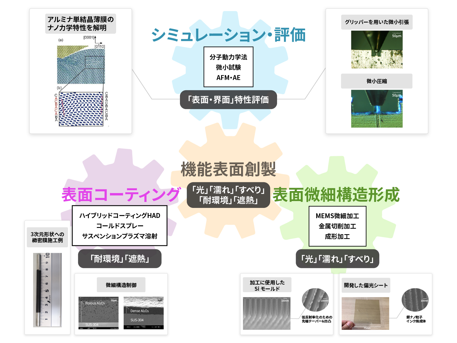
Our research involves integrating ”surface microstructure formation”, "surface coating," and "simulation and evaluation technologies" to create highly functional surfaces capable of controlling "light", "wettability", "slipperiness", "environmental resistance", and "thermal barrier properties".
We have established a system that enables researchers with knowledge in various fields to work together in an integrated manner, and are engaged in consistent activities from the elucidation and proposal of surface functional physical phenomena to actual processing and evaluation, leading to their implementation in society.
Keywords
MEMS microfabrication, metal cutting, forming, hybrid coating, HAD, cold spray, molecular dynamics, micro-testing, AFM/AE, highly durable wire grid polarized sheets.
Subjects
-
1.Surface Microstructure Formation
We create functional surfaces with controlled wettability, optical properties, and slipperiness by forming surface microstructures using MEMS microfabrication technologies such as nanoimprinting, metal cutting and forming technologies.
-
2.Surface Coatings
By developing coating technologies with controlled film quality, from porous to dense films on complex shapes, through the advancement of hybrid coating HAD and cold spraying, we will create functional surfaces with excellent environmental and thermal barrier properties.
-
3.Simulation and Evaluation
Contribute to the design of functional surfaces by advancing evaluation techniques that lead to the elucidation of nanomechanical properties of materials and surface functional physical phenomena through the use of molecular dynamics, micro-testing, and AFM/AE.
Themes
-
Highly durable wire grid polarizing sheets
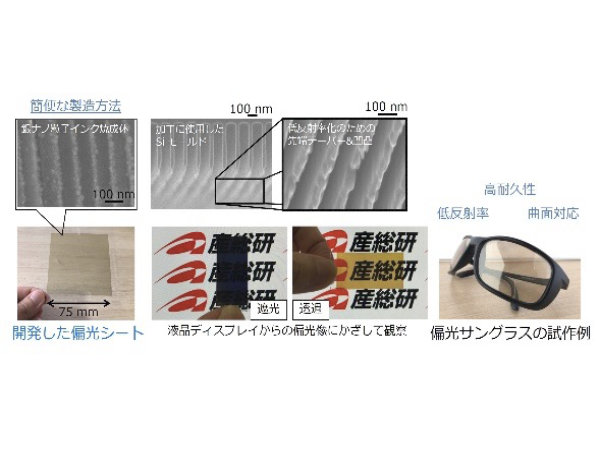
- ●Nano-imprinting and metal-embedding technologies enable WG polarizing elements with low reflectivity and high durability
- ●High heat/moisture/light resistance, unique low reflectance structure, and curved surface shape compatibility differentiate WG polarizers.
- ●R&D is in progress for further enhancement of functionality.
-
Hybrid Coating Technology
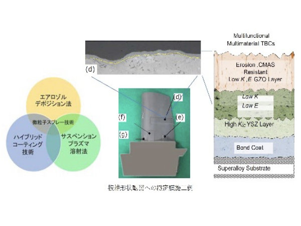
- ●Interface controlling that enables Multi-layer technology for different types of coatings.
- ●Surface functionalization of three-dimensional complex shapes and porous materials.
- ●Different functions can be added (ex. thermal barrier and encapsulation).
-
Development of Advanced Ceramic Coating Technology
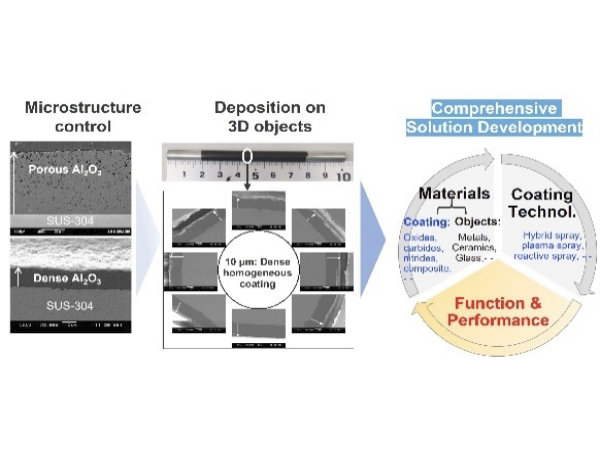
- ● SiC coating with strong adhesion by Hybrid aerosol deposition
- ● AlN coating with bulk like properties by fine particle spraying
- ● Microstructural control & coating design to realize the required function on 3D objects
- ● Comprehensive development from starting powder, suitable coating technology to
realize the required function & performance
-
Mechanical property evaluations using micro-sized specimens
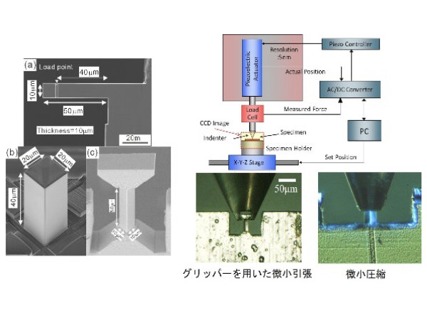
- ●Site specific mechanical property evaluation utilizing focused ion beam machining.
- ●Evaluation of mechanical properties under variable stress conditions including bending, compression and tension.
- ●A wide range of scales, from tens of microns to nanometers, can be evaluated.
-
Nanomechanical Characterization Technology.
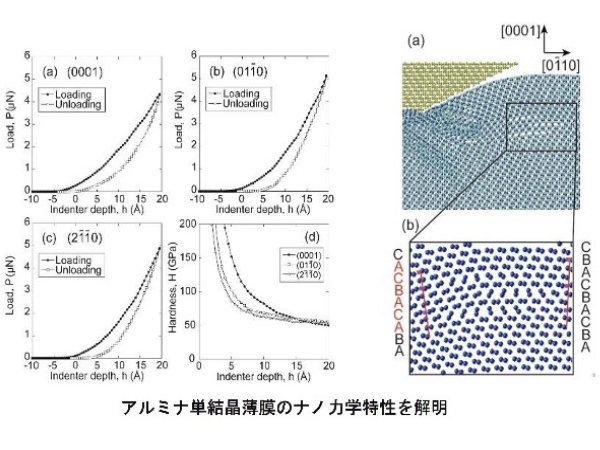
- ●Molecular dynamics techniques are used to understand the mechanism of mechanical properties of materials from a nanoscale perspective.
- ●Analysis and evaluation of deformation and structural changes based on electrons/atoms.
- ●Utilization of the most advanced computing technologies such as data science.
-
Detection of AE signals in SPM
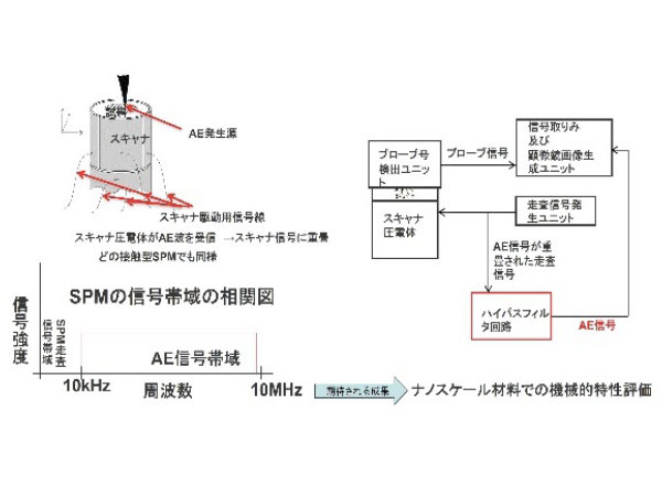
- ●Reception of AE waves caused by friction and wear in the SPM by the scanner piezoelectric element.
- ●AE signals are superimposed on the scanning signal of the scanner piezoelectric element and detected simultaneously with the probe signal.
- ●AE signals are detected from analysis of probe and scanning signals without sensors.
-
Development of functional components using nanostructured materials.
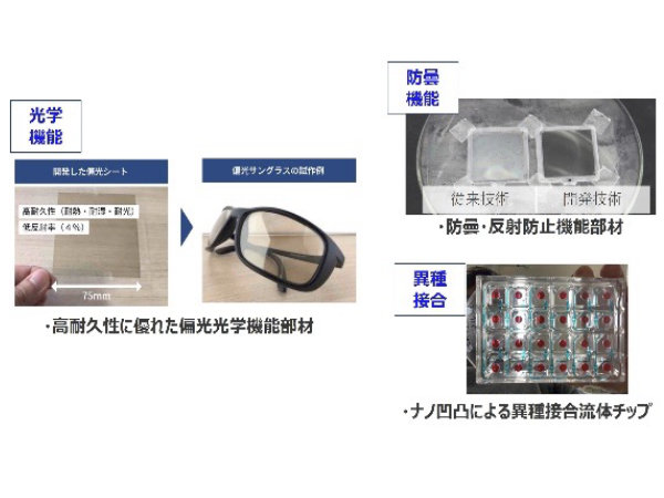
- ●World's highest level of optical functions with excellent environmental resistance, such as anti-reflection and polarization functions.
- ●Dissimilar bonding technology with reduced deformation during bonding.
- ●Realization of wetting control technology.
- ●The only company in the world that has established anti-reflective lens formation technology using only injection molding technology with excellent mass production capabilities.