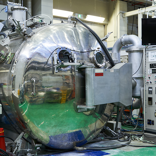
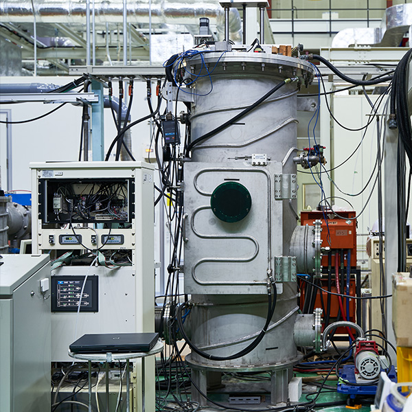
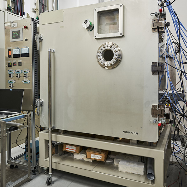
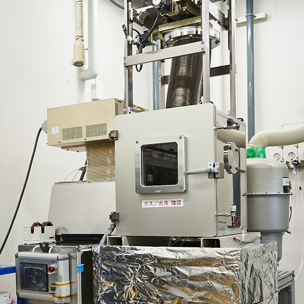
Microstructure Processing Equipment
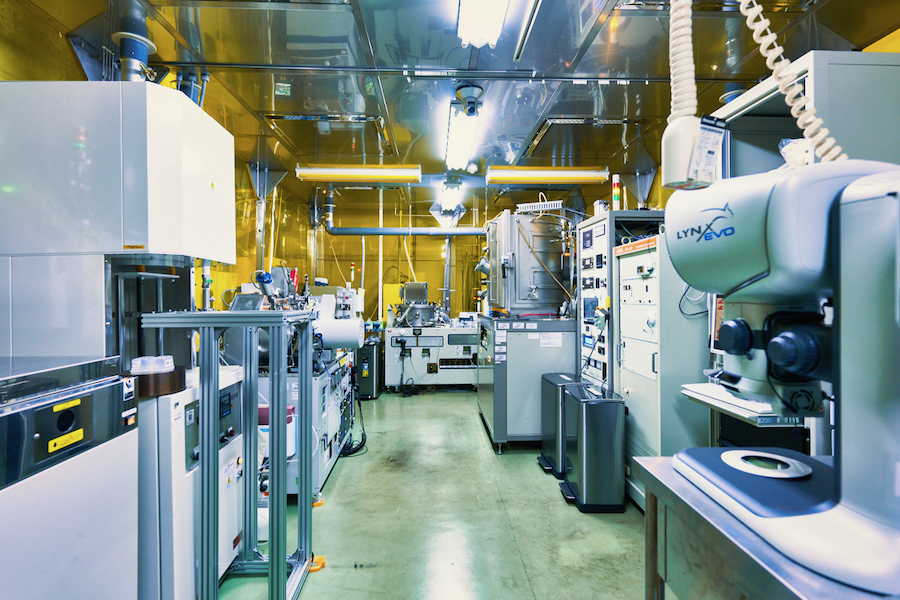
- 3-way RF magnetron sputtering system (No.1)
- 3-way RF magnetron sputtering system (No. 2)
- EB evaporation system
- Parallel plate reactive etching system
- Magnetic induction reactive etching system
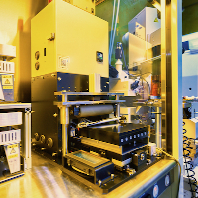
- UV nanoimprint lithography system
- Projection aligner
- Double-sided aligner
- Spin coater
- Screen printer
- Magnetizers
- Vacuum rotary/rotary mixer
- Non-electric field plating machine
- Electric field plating machine
- multi-layer dip coating equipment
- Vacuum heating furnace
- Vacuum drying furnace (No. 1)
- Vacuum drying furnace (No. 2)
- Vacuum drying furnace (No. 3)
- Cooling furnace
Metal and resin processing equipment
- Injection molding machine
- Large-area nanoimprinting equipment
- Cutting machine
- Tool scraping equipment
- Biaxial mixing machine
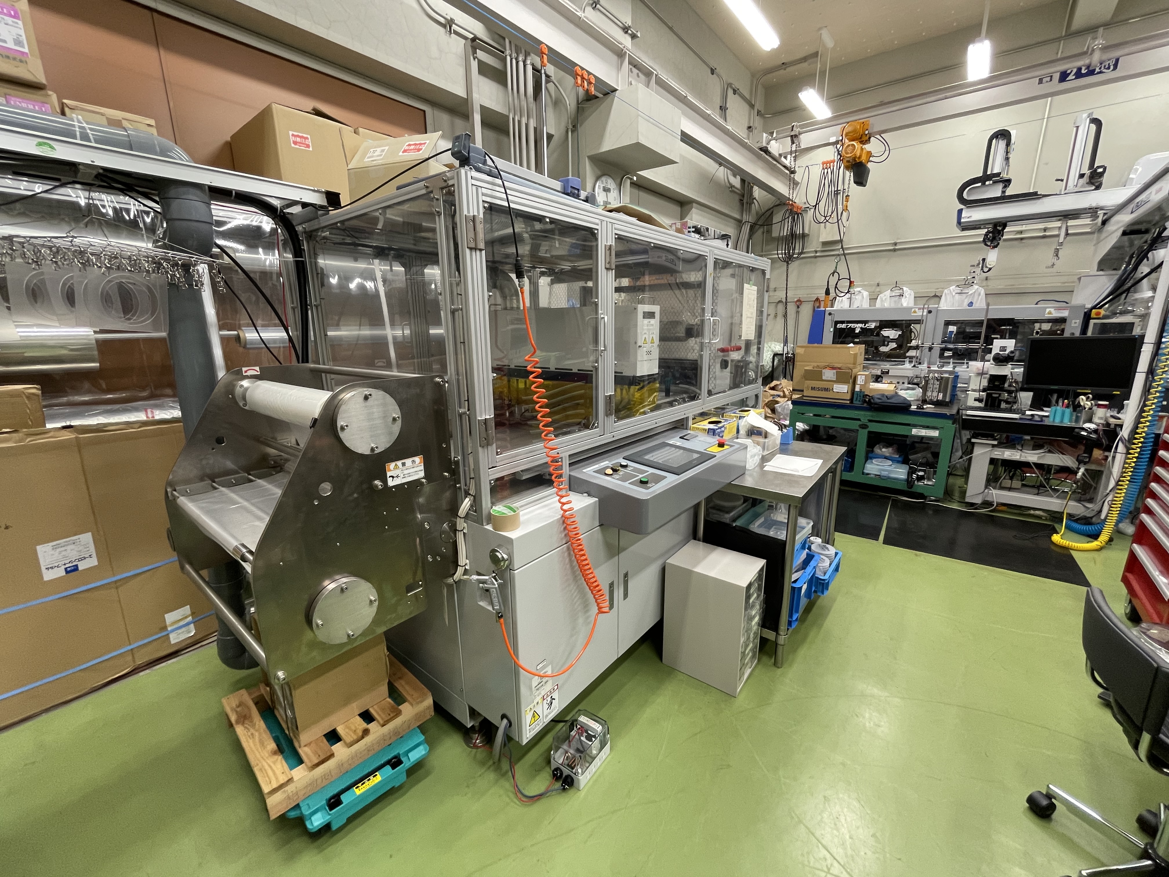
- Film extrusion machine
- Pelletizer
- Mixer
- Resin dryer
- Pulverizer
- Weighing and mixing machine
- CO2 laser cutting machine
- Thermo-compression bonding equipment
- Corona treatment machine
- 3D printer (No. 1)
- Large-scale 3D printer (No. 2)
- 3D printer (No. 3)
Evaluation equipment
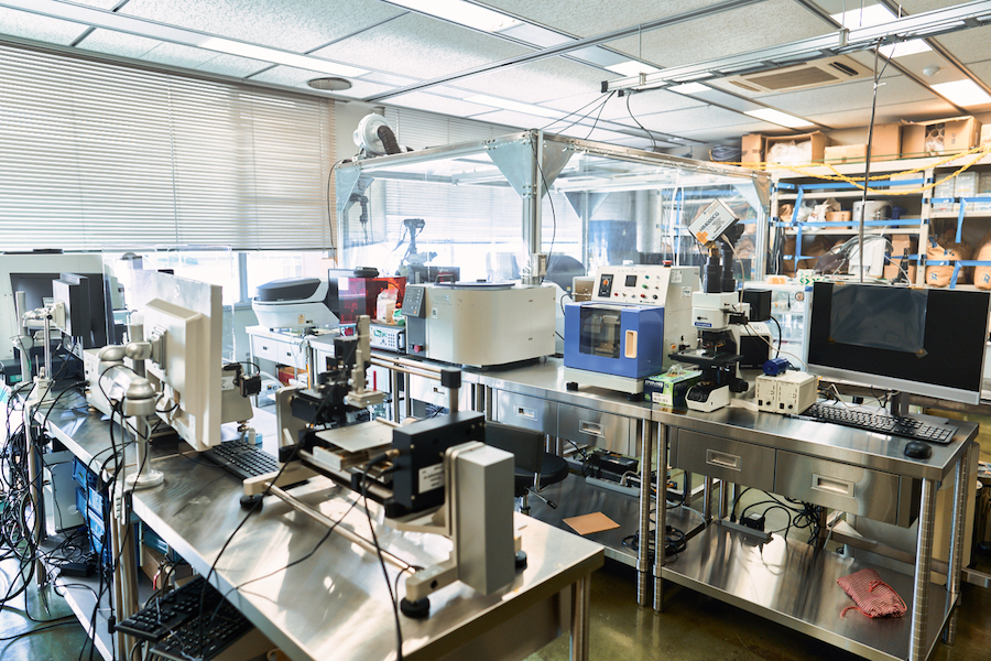
- Energy dispersive X-ray analyzer (EDX)
- Large UV/Visible spectrophotometer(No.1)
- Large UV/Visible spectrophotometer(No.2)
- Scanning probe microscope (AFM)
- Tentacle surface profiler (DEKTAK)
- Fourier transform infrared spectrophotometer (FTIR)
- Differential scanning calorimeter (DSC)
- Thermogravimetry (TGA)
- Laser microscope
- Microtome
- Cross-section polisher
- Contact angle measuring device
- Friction Force Measuring Equipment
- High-temperature humidification tester
- Microscopic and visible spectrometer for lenses
- Microscopic Spectrometer
- Vacuum Electron Dyeing Equipment
- Vacuum Electron Dyeing Equipment
- Polishing machine
- Magnetizers
- Shaker
- Optical microscopes
- Stereo microscope
- 3D Imaging Type Stereo Microscope
- Microscopes
- Optical evaluation equipment (surface plate, etc.)
Original equipment designed and manufactured by AIST
-
UV nanoimprint lithography equipment
UV nanoimprint lithography equipment is used to perform nano-lithography using UV nanoimprint. We perform nanometer-order lithography on the surface of 8-inch wafers to fabricate molds.
-
Electroless plating system
This is an automatic electroless plating system that performs thick nickel plating for optical lens molds on the surface of heat insulating materials and metal molds. We have performed electroless nickel plating of 200-300μm thickness on the surface of mainly heat insulating materials and standard metal molds to produce optical lens pieces.
-
Film Extrusion Molding Machine
This machine forms 350mm wide continuous films. We have been engaged in the research and development of high-functional surface components combining materials and structures by integrating biaxial blending machines and fine nano-transcription technology.
-
Thermal welding machine
This machine forms 350mm wide continuous film. We have been engaged in the research and development of high-functional surface components combining materials and structures by integrating our biaxial mixing machine and fine nano-transcription technology.
-
Multi-layer Dip Coating System
This system automatically processes multiple solutions according to a pre-programmed schedule. We use this equipment for the development of coating technology using multiple solutions.
Hybrid Coating
-
Multi-purpose Large-scale Coating System
This is a multi-purpose coating system equipped with an industrial robot in a large chamber of 2 m class. We can handle everything from 3D-driven hybrid AD systems to cold spraying.
-
Decompression plasma spraying system
40 kW class DC plasma spraying system that can be applied under reduced pressure.
-
Hybrid AD system (general-purpose)
Hybrid coating system for prototyping ceramic coatings, equipped with a 5-axis stage and capable of applying coatings to three-dimensional objects.
-
Hybrid AD equipment
Hybrid coating equipment for prototyping of ceramic coatings.
-
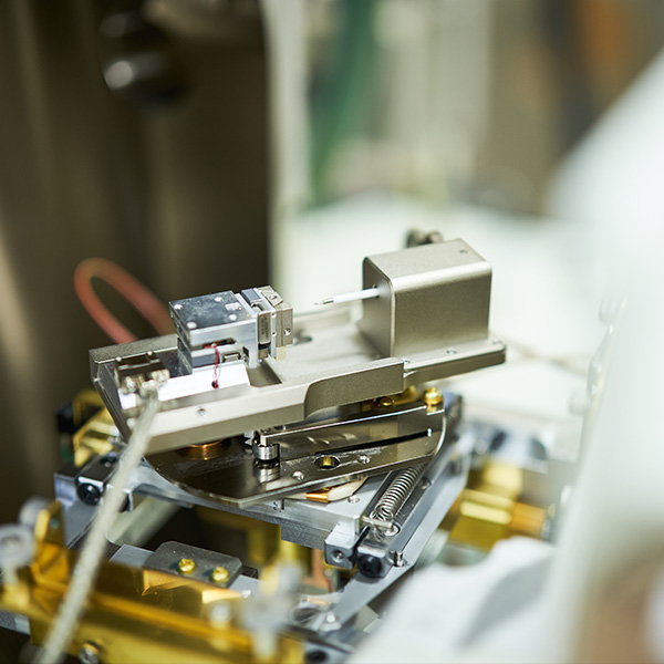
Nanoindenter equipment in SEM
This is a nano-indenter that enables evaluation of micromechanical properties in scanning electron microscope.
