Power Device Application Design Team
Our objective is to cultivate new application fields by utilizing the high-voltage SiC devices and packages. we are also promoting the creation of crystal defects inspection platform and the preparation of international standard draft, which directly affect the reliability of wide bandgap semiconductor devises.
Proprietary technology
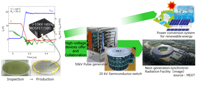
- High-voltage (>10 kV) SiC-MOSFET/SBD device technology
- Crystal defects evaluation/analysis technology for wide bandgap semiconductor
Priority Research
- Prototype supply of high-voltage SiC-MOSFET/SBD devices for power converter applications
- Standardization of defect inspection methods and device reliability for compound semiconductor wafers
Major Patents and Publications
- “13 kV SiC-DMOSFETs and body diodes for HVDC MMC converters”, Koji Nakayama, Takeharu Kuroiwa and Hiroshi Yamaguchi, Japanese Journal of Applied Physics 61, 014001 (2022).
- “Influence of SiC epitaxial wafer quality on yield of 1.2kV SiC-DMOSFETs”, Junji Senzaki, Ryoji Kosugi, Keiko Masumoto, Takeshi Mitani, Takeharu Kuroiwa and Hiroshi Yamaguchi, Proceedings of IEEE International reliability physics symposium 2022, in press.
- “Recent Progress of Silicon Carbide Super-Junction MOSFETs”, Ryoji Kosugi, Shiyang Ji, Kazuhiro Mochizuki, Takeharu Kuroiwa and Hiroshi Yamaguchi, Extended abstract of International Conference on Solid State Devices and Materials 2020 D-6-01.