Power Device Research Team
We are developing high-performance and high-reliability power devices with the aim of expanding the use of wide-gap semiconductor power devices. In particular, we aim to be the first in the world to demonstrate the performance of new devices using SiC and GaN as substrate materials, and to create fundamental technologies that will lead to breakthroughs.
Team's research agenda or results, etc.
Research on SiC power devices
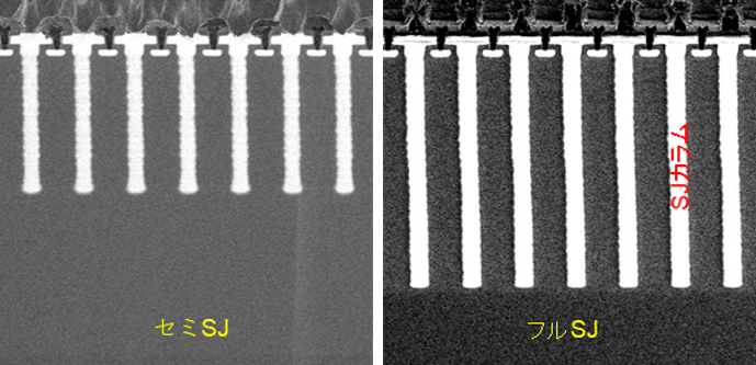
We are working on SiC power devices with low ON-resistance and high reliability as key issues for their full-scale commercialization. We have successfully implemented planar-gate and trench-gate MOSFETs in society, and have developed new devices such as SWITCH-MOS, a unique structure of Schottky-embedded MOSFETs. In recent years, we have been developing the world's first super junction MOSFETs with even lower ON-resistance.
Research on SiC power ICs
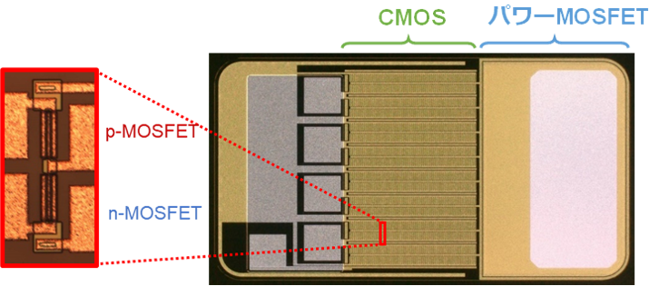
Further loss reduction of SiC power devices requires a reduction of switching loss due to high-speed switching. We believe that high-speed control will be possible if the gate driver that drives the power device can be integrated. We are developing SiC monolithic power ICs that integrate SiC CMOS driver circuits and vertical power devices on the same chip.
Research on GaN power devices
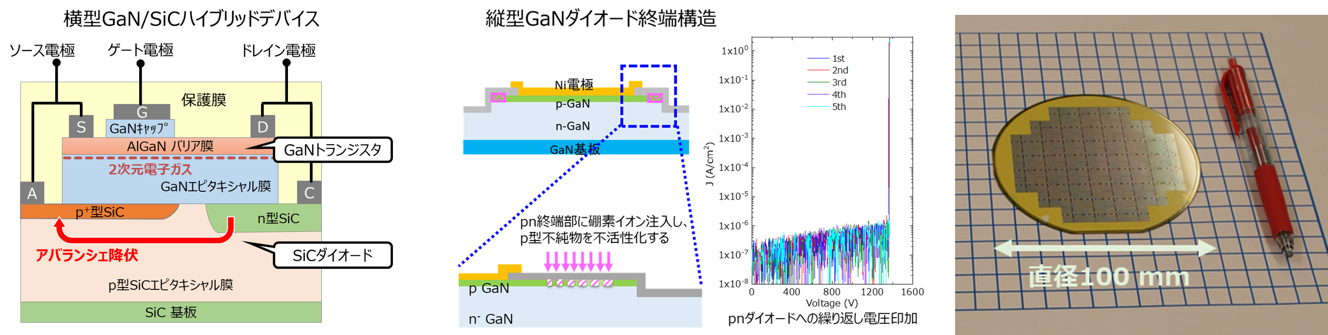
GaN semiconductors are expected to have high conduction and high-speed switching characteristics, but they are vulnerable to voltage because they lack the pn termination structure required for power devices, so they have not been deployed in applications requiring high reliability, such as automotive applications.
Research on MOS interface control
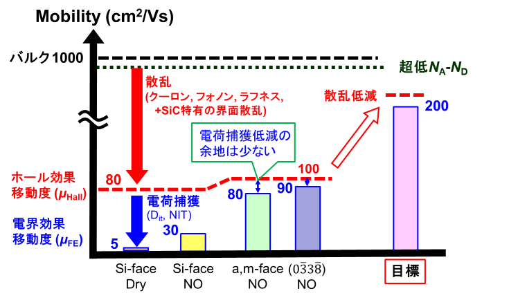
The key process in SiC and GaN power MOSFET fabrication is MOS gate oxide film formation. We have clarified the relationship between MOS interface traps and channel electron density as the rate-limiting factor for channel mobility in SiC-MOSFETs. In the future, we will also clarify the scattering mechanism of mobile electrons and develop a gate oxide film formation process that suppresses scattering. We plan to apply our findings to next-generation materials such as GaN.