Diamond Wafer Research Team
We are conducting research and development aimed at social implementation of diamond based on high-quality and large (> cm to inch) diamond wafer fabrication technology and electronic device technology.
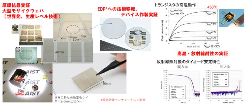
Proprietary technology
- Large wafer
- Device fabrication and measurement
- Crystal Evaluation
- (CVD system) Simulation
Priority Research
- Larger wafer diameter
- Device Demonstration
Major Patents and Publications
- “A 2-in. mosaic wafer made of a single-crystal diamond” , H. Yamada, A. Chayahara, Y. Mokuno, Y. Kato, Applied Physics Letters 104 (2014), article number 102110; https://doi.org/10.1063/1.4868720
- “Method to increase the thickness and quality of diamond layers using plasma chemical vapor deposition under (H, C, N, O) system”, H. Yamada, A. Chayahara, Y. Mokuno, Diamond and Related Materials 101 (2020), article number 107652; https://doi.org/10.1016/j.diamond.2019.107652
- “Recent advances in diamond power semiconductor devices”, Materials Science in Semiconductor Processing 78 (2018), pp. 147-156, H. Umezawa; https://doi.org/10.1016/j.mssp.2018.01.007
- “Large reduction of threading dislocations in diamond by hot-filament chemical vapor deposition accompanying W incorporations”, S. Ohmagari, H. Yamada, N. Tsubouchi, H. Umezawa, A. Chayahara, S. Tanaka, and Y. Mokuno, Appl. Phys. Lett. 113 (2018) 032108; https://doi.org/10.1063/1.5040658