Wafer Process Research Team
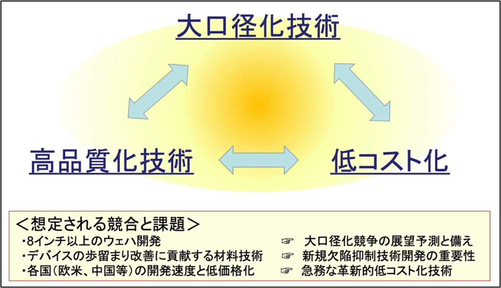
The Wafer Process Team mainly conducts research and development of manufacturing technology for SiC bulk single crystals for power semiconductors and wafer processing technology. The three conditions of large diameter, high quality, and low cost are required for wafer materials, and we aim to create next-generation material technologies by collaborating with the four technical fields of materials, equipment, processes, and evaluations that combine these from crystallography to materials engineering and precision engineering.
Priority Research
Research on crystal growth (sublimation method)
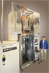
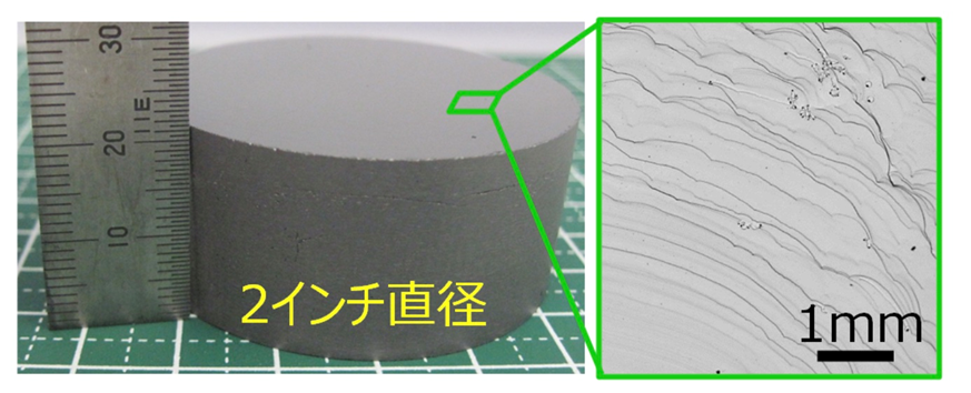
Sublimation growth of SiC is when a SiC raw material powder is sublimated in a graphite crucible at a high temperature of 2,000 degrees Celsius or more and a single crystal growth is performed by gas phase transport. We have multiple large and small high-frequency heating furnaces, and we are developing high-speed growth technologies that will lead to large-diameter growth of more than 6 inches and cost reduction.
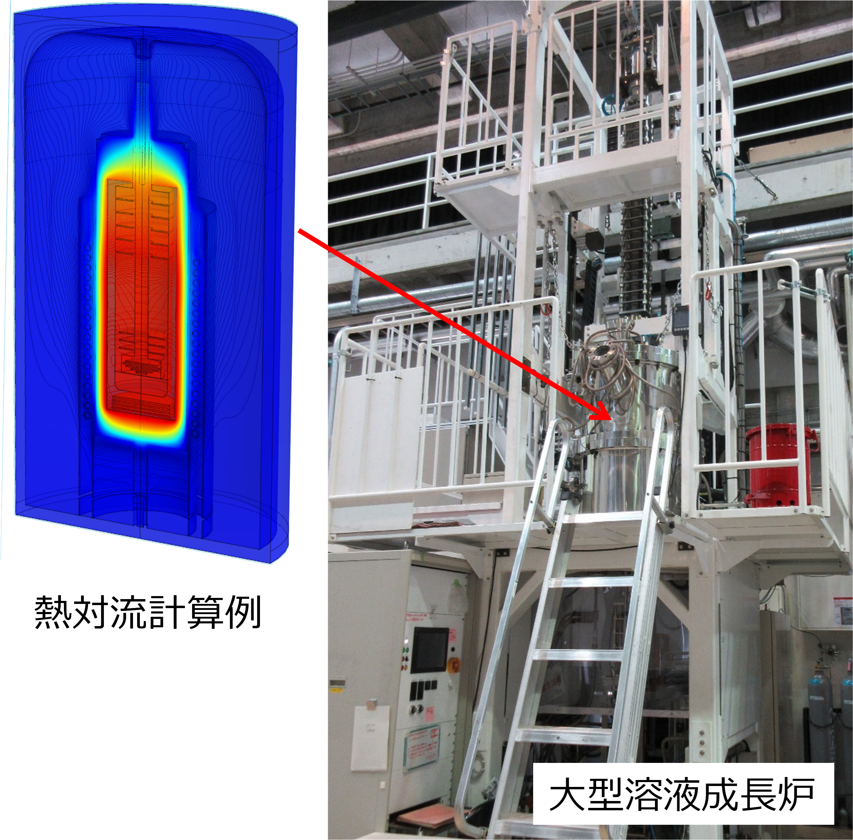
Research on crystal growth (solution method)
The solution growth method is to precipitate SiC from a high-temperature solution containing Si and C heated to about 2000°C. In principle, this method is advantageous for the cultivation of high-quality crystals with low defect density, and is expected to be a new crystal growth method. The research and development of this growth method is to suppress the roughness of the growth interface called step bunching while increasing the SiC growth rate by increasing the C concentration in the solution.
Wafer Processing Research
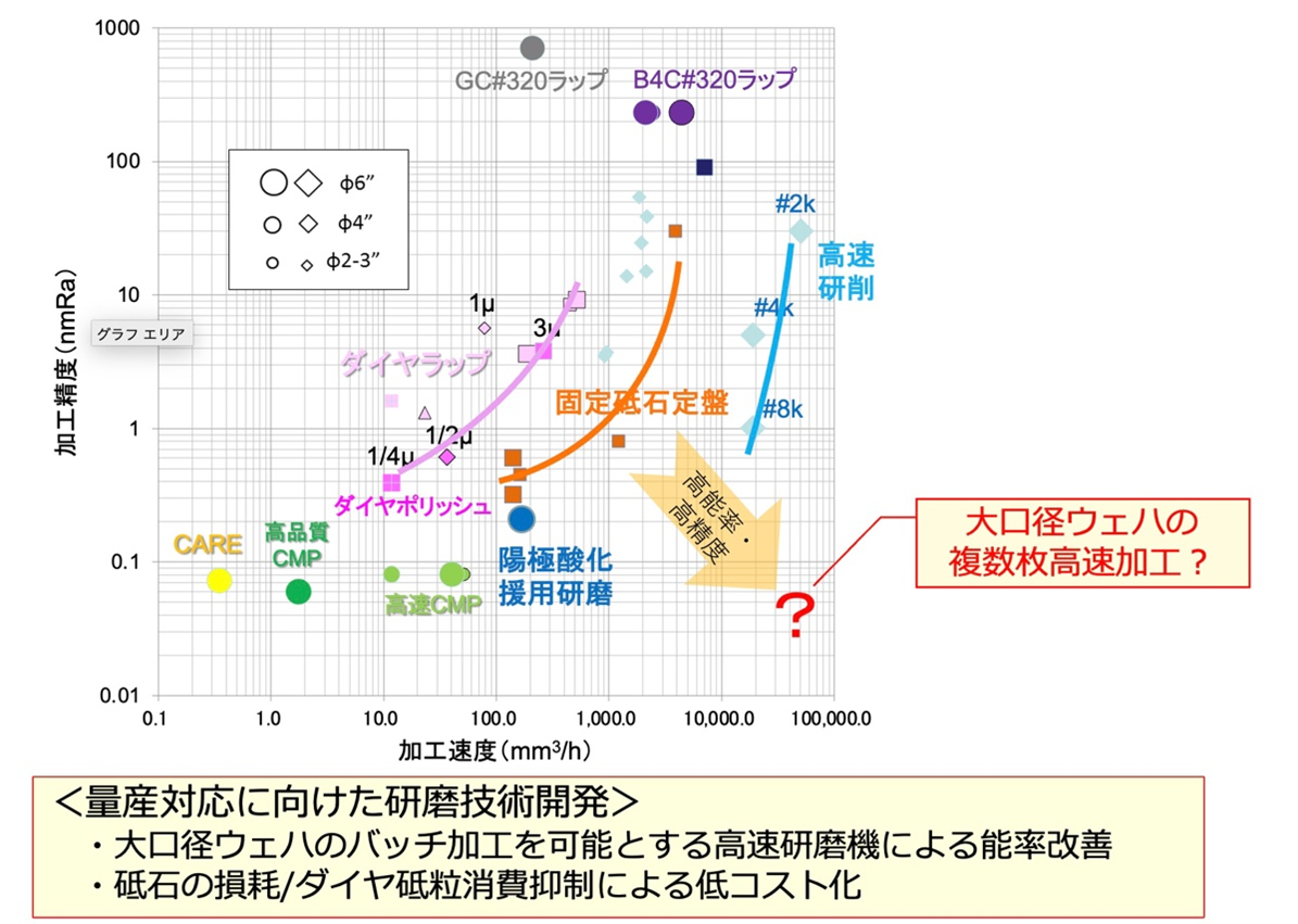
Hard and brittle SiC single crystals are a long and costly process to process into wafers. Processes such as cutting, polishing and grinding require expensive diamond abrasives.
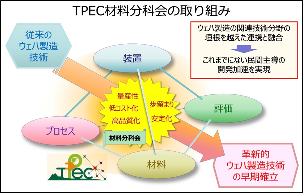
Promotion of industry-academia-government collaboration development at TPEC
In 2019, we established a new materials subcommittee at TPEC, a private-sector collaborative research organization. (details here) Mainly, by interconnecting research and development on SiC bulk single crystal growth, wafer processing technology, and wafer evaluation technology, We aim to establish a world-first SiC wafer mass production technology that achieves both large aperture, high quality, and low cost.
Keep the technology
- Large diameter SiC growth
- High-speed SiC growth
- High Concentration Impurity Doping SiC Growth Technology
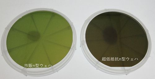
- Low resistance n-type and p-type SiC bulk single crystal growth
- Low-defect SiC growth technology
- Large-diameter SiC high-speed processing technology
- Wafer evaluation technology
Major Patents and Publications
- K. Eto, H. Suo, T. Kato, H. Okumura,“Growth of P-type 4H–SiC single crystals by physical vapor transport using aluminum and nitrogen co-doping”, J. Cryst. Growth, 470, (2017) 154–158. https://doi.org/10.1016/j.jcrysgro.2017.04.025>
- H. Suo, K. Eto, T. Ise, Y. Tokuda, H. Osawa, H. Tsuchida, T. Kato, H. Okumura, “Difference of double Shockley-type stacking faults expansion in highly nitrogen-doped and nitrogen-boron co-doped n-type 4H-SiC crystals”, J. Cryst. Growth, 468, (2017) 879–882. https://doi.org/10.1016/j.jcrysgro.2016.12.055
- T. Kato, K. Eto, S. Takagi, T. Miura, Y. Urakami, H. Kondo, F. Hirose, H. Okumura, “Growth of low resistivity n-type 4H-SiC bulk crystals by sublimation method using co-doping technique”, Mater. Sci. Forum, 778-780, (2014) 47-50. https://doi.org/10.4028/www.scientific.net/MSF.778-780.47
- Takeshi Mitani, Kazuma Eto, Kenji Momose, Tomohisa Kato, “Massive reduction of threading screw dislocations in 4H-SiC crystals grown by a hybrid method combined with solution growth and physical vapor transport growth on higher off-angle substrates”, Applied Physics Express, 14 (2021) 085506. https://doi.org/10.35848/1882-0786/ac15c1
- Takeshi Mitani, Naoka Komatsu, Tomohisa Kato, "Relationship between macrostep shape and solvent composition in 4H-SiC solution growth", Journal of Japan Society for Crystal Growth, Vol. 45(2018)45-2-02 https://doi.org/10.19009/jjacg.3-45-2-02.
- Takeshi Mitani, Naoyoshi Komatsu, Tetsuo Takahashi, Tomohisa Kato, Shunta Harada, Toru Ujihara, Yuji Matsumoto, Kazuhisa Kurashige, Hajime Okumura, “Effect of aluminum addition on the surface step morphology of 4H-SiC grown from Si-Cr-C solution”, Journal of Crystal Growth, 423 (2015) 45. https://doi.org/10.1016/j.jcrysgro.2015.04.032
- Takeshi Mitani, Naoyoshi Komatsu, Tetsuo Takahashi, Tomohisa Kato, Kuniharu Fujii, Toru Ujihara, Yuji Matsumoto, Kazuhisa Kurashige, Hajime Okumura, “Growth rate and surface morphology of 4H-SiC crystals grown from Si-Cr-C and Si-Cr-Al-C solutions under various temperature gradient conditions”, Journal of Crystal Growth, 401 (2014) 681. https://doi.org/10.1016/j.jcrysgro.2013.11.031
- Tomohisa Kato, "Overview: Processing Technology for SiC Wafers for Power Devices"、Journal of the Japan Society for Abrasive Technology Vol.61 No.8 (2017) 418-421.
- Patent No. 6755524 "Method for producing p-type 4H-SiC single crystal and p-type 4H-SiC single crystal"
- Patent No. 6757955 "n-type SiC single crystal substrate and method for producing the same, and SiC epitaxial wafer" method"