Fabrication Engineering Research Team
The center is mainly engaged in joint research with TPEC (Tsukuba Power Electronics Constellations), an open innovation platform, and other organizations, and is developing technologies for device mass production and elemental processes by utilizing the 4-inch wafer power device prototyping line in the West 5D building, which is managed and operated by the center. The center is also developing technologies for device mass production and elemental process technologies. The prototype device chips are also provided to various applications.
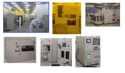
Technology and Equipment
Equipment
- Tsukuba West Plant, Building 5D, 4-inch SiC/GaN wafer power device prototyping line
Technology
- SiC film epitaxial growth technology: low concentration control, thin film to thick film growth technology, multi-stage regrowth technology
- High-temperature ion implantation technology (for SiC wafers): Al, N, P implantation, 350 keV max
- Photolithography technology: i-line stepper (0.5μm), g-line stepper
- Dry etching techniques: SiO2-RIE, SiC-ICP, Poly-RIE, GaN-ICP, TiN/Ti/Al-RIE, O2 ashing
- Insulating film formation technology: Thermal CVD (NSG/PSG), PE-CVD (SiO2), thermal oxidation (Dry-O2, NO)
- Gate formation technology: LP-CVD P-doped Poly-Si, HTO
- Wet etching technology: Al, Ni, Ti, SiO2
- Cleaning techniques: SPM, RCA, DHF, resist stripping
- Metal technologies: Sputtering (Al, Al-Si, Ni, Ti, TiN), Evaporation (Ti, Ni, Au), W-CVD (under consideration)
- Heat treatment techniques: activation annealing, electrode annealing (sinter)
Prototype devices available from the AIST-West 5D fabrication-line
Equipment
- SiC SBD(1.2kV)
- SiC PN Diode
- SiC IE-MOSFET
- SiC IE-UMOSFET (1.2kV)
- SiC SJ(Super Junction) structure
- SiC SWITCH-MOSFET
- SiC DMOSFET
- SiC CMOSFET
- GaN PN DIODE
- GaN UMOSFET
- GaN HEMT