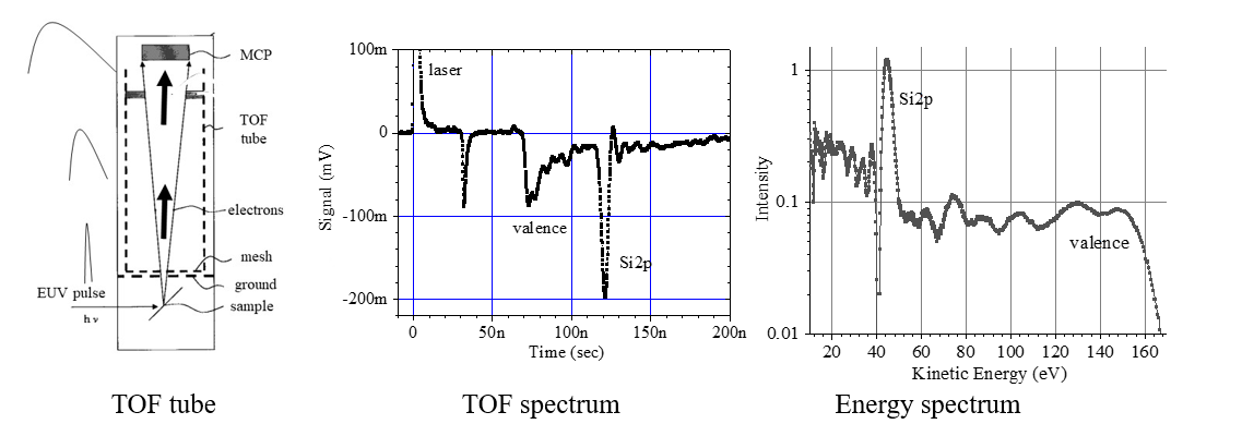


Photoelectron Spectroscopy with a Pulsed EUV Source(EUPS) EUPS is a photoelectron spectroscopy system, in which an EUV pulse (255.17 eV, 3-ns duration) emitted from a laser-produced plasma excites a sample and the energy spectrum of electrons is analyzed with a time-of-flight (TOF) analyzer. The principle of EUPS was invented and many technologies for implementing the EUPS were developed at AIST.1
Equipment
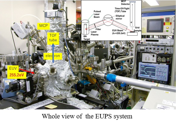
Photoelectron Spectroscopy with a Pulsed EUV Source (EUPS)
A high-power short-pulse laser is focused on a BN round bar target to generate a high-temperature plasma. The emission line at 255.17 eV from boron ions in the plasma is focused on a sample with an elliptical mirror. The electrons emitted from the sample travel in a flight tube, and the time taken to arrive at an electron detector is converted into kinetic energy to obtain the energy spectrum.
Sample holder
4 samples (10 mm × 3 mm) can be loaded. Powder samples can be measured. Maximum size of sample: 20 mm × 20 mm. Temperature dependence from RT to 400 °C. Pre-treatment: sputtering, heating up to 1,000 °C in gas atmosphereApplications
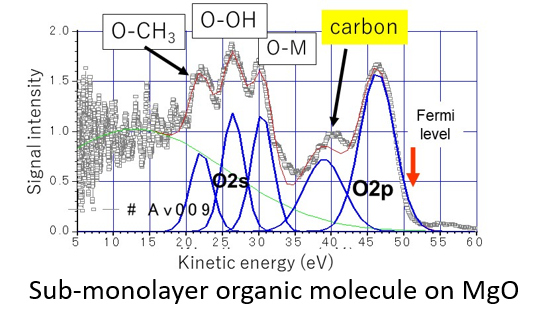
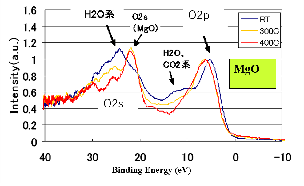
・Analysis of the electronic states of the outermost atomic layer (about 0.5 nm) of a solid sample including a powder sample.
・Evaluation of the diffusion of elements from the lower layer to a nanometer-thin film.
・Measurement of insulating and organic thin films while suppressing charging.
・Evaluation of oxygen vacancies.
・Evaluation of the band bending of semiconductors.
・Evaluation of the work function of insulators, the conductivity of powder samples, the electron energy relaxation time, and the amount of charge trap centers using a secondary electron spectrum.
Principle and Features
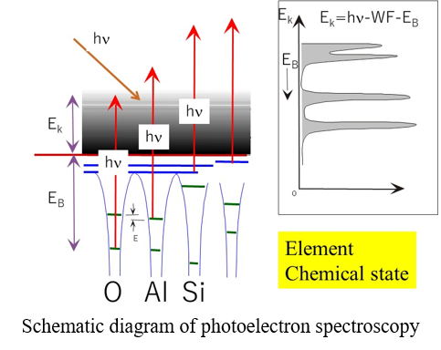
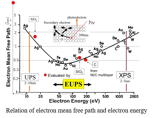
Photoelectron spectroscopy, which obtains the energy spectrum of photo-emitted electrons, provides information on the electronic states of the surface.・In EUPS, the photon energy of the excitation light is 250 eV and the kinetic energy of the photoelectrons is in the energy region where the electron escape depth is the shallowest at 0.5 nm, so it has ultra-high sensitivity for detecting impurities of one atomic layer or less.
・Utilizing the pulse nature of the light source, the electron energy is analyzed by the time-of-flight (TOF) method. Since electrons in the entire energy region are measured at the same time, a wide spectrum can be obtained with a small number of irradiations.
・Thanks to this feature, the charging of insulators is minimized, and so the work function of insulators can be measured.
・Since the brightness of the light source is extremely high and the instantaneous photon density on the surface is very high, the resistance of an ultra-thin film can be evaluated. Band bending and charge trap centers having a lifetime of milliseconds or less can also be evaluated from the dependence of the electron spectrum on the excitation intensity.
Examples
・Analyses using a secondary electron spectrum
In TOF, a spectrum in a wide energy region is obtained with only oneshot EUV irradiation.
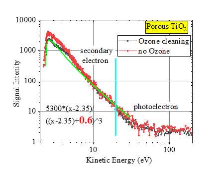
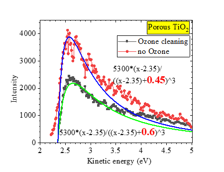
Detection of changes of the properties of TiO2 nanocrystals by ozone cleaning of the Si substrate
4 samples: Porous and compact TiO2 with and without ozone cleaning of the Si substrate
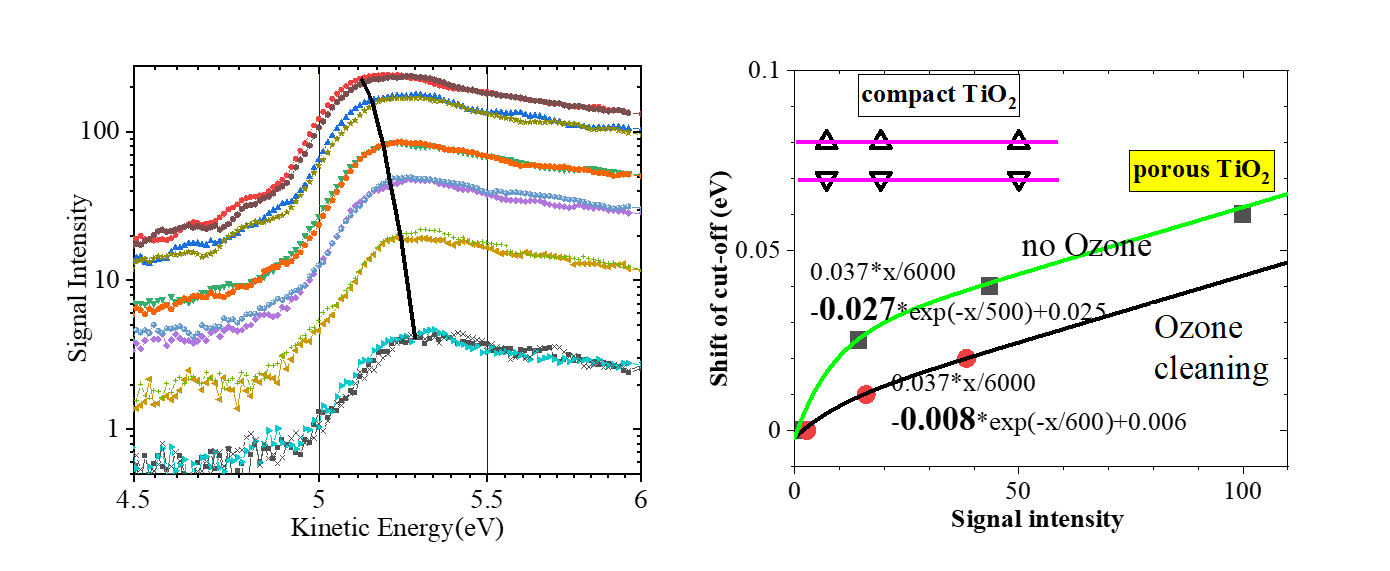
Effect to the density of charge traps
The shift of the cut-off position, as seen in the left figure, gives: a) the resistivity of a sample from the slope, and b) the density of charge trap centers from the rapid saturation at low intensity. The right figure shows that, in nano-porous TiO2, the number of charge trap centers was reduced by ozone cleaning.
Effect to lifetime of excited electronsThe spectral shape near the cut-off reflects the energy relaxation time of excited electrons. In porous TiO2, ozone cleaning increased the lifetime, indicating that the density of defects was reduced.
Applications using high surface sensitivity
Evaluation of contamination on a protective oxide for a plasma display
EUPS has high surface sensitivity for detecting sub-mono atomic-layer contamination owing to a small photoelectron escape depth of about 0.5 nm. Detection by EUPS of a very small amount of contaminants on a protective oxide of a plasma display panel, which was difficult to measure with ordinary XPS, led to identification of the contamination source, and the
manufacturing process was improved.
Other examples
・Band bending of Si wafer was measured.
・Temperature dependence of the work function of insulating materials such as glass and alumina was measured.
・It was found that Si does not diffuse into TaN and W nano-thin films, but diffuses in large amounts in TiN, and that the diffusion of Hf in TiN changes significantly with the addition of O or Al.
・It was found that the temperature at which the conductivity of the exhaust gas purification powder catalyst increases coincides with the temperature at which the catalytic activity increases.
・Correlation between the inclination angle of the electron cloud on the surface of the powder catalyst and the catalytic activity was measured.