
Scanning Electron Microscope with a Superconducting Tunnel Junction X-ray Detector(SC-SEM) The scanning electron microscope with a superconducting tunnel junction X-ray detector (SCSEM)is an SEM-EDX analyzer that features both the high throughput (10?3 sr) of semiconductor X-ray detectors and the high energy resolution (<10 eV) of wave-dispersive X-ray detectors (WDS). The SC-SEM is useful for nondestructively obtaining spatial information on the elemental composition of a sample.
Equipment
Scanning electron microscope with a superconducting tunnel junction X-ray detector (SC-SEM)
・X-ray detector: Superconducting tunnel junction X-ray detector + Polycapillary X-ray lens
・SEM: JSM-IT800SHLs (JEOL)
Applications
・Analysis of trace light elements contained (> 100 ppm) in semiconductor materials and structural materials
・2D mapping of lithium (Li).
・Oxidation state analysis of transition metals such as iron (Fe) and copper (Cu)
・Nanometer-scale elemental mappingPrinciple and Features
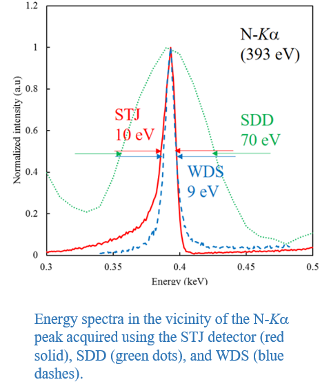
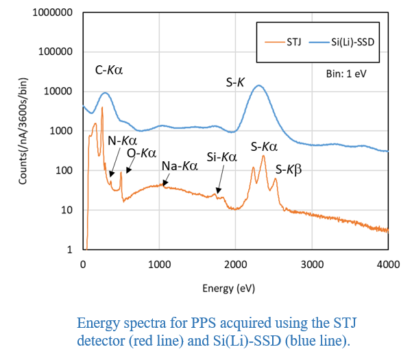
・The energy dispersive X-ray detector based on the STJ exhibits both the high throughput of semiconductor X-ray detectors and the high energy resolution of wavelength-dispersive X-ray spectrometers (WDSs). The STJ X-ray detector can clearly distinguish the K-lines of light elements from the L- and M-lines of various elements and can detect Li-Kα (54 eV) due to its high sensitivity for low energy.
・X-ray detection performance
・X-ray detection energy range: 40 eV - 4 keV
・Energy resolution: approximately ~7 eV at 400 eV X-ray
・Maximum counting rate: 200 kcps・Scanning electron microscope: JSM-IT800SHLs (JEOL)
・Accelerating voltage range: 10 V - 30 kV
・Electron beam spot size: 0.6 nm at 15 kV, 1.1 nm at 1 kV.
・Maximum sample size: Φ100 ㎜、Φ10 ㎜ (diameter)
Examples
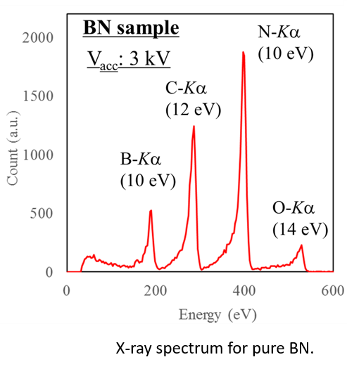
・Elemental analysis of boron nitride (BN)
・The X-ray spectrum acquired by using the SC-SEM for a BN powder is shown in the right figure. Separate B-Kα (188 eV), C-Kα (277 eV), N-Kα (393 eV), and O-Kα (525 eV) peaks can be clearly observed due to the high energy resolution. The C-Kα and O-Kα peaks originated from carbon compound materials and an oxidized layer on the surface of the BN, respectively.
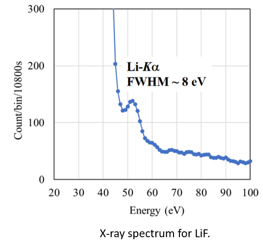
・Elemental analysis of a lithium fluoride (LiF)
・The X-ray spectrum acquired by using the SC-SEM for a LiF crystal is shown in the right figure. Li-Kα (54 eV) peaks can be detected due to the high sensitivity for low energy. The energy resolution of Li-Kα was approximately 8 eV.
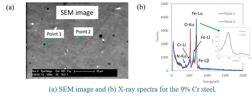
・Light elements (B, C, N, O, etc.) have a large influence on the performance of structural materials, such as highresistance steels. To understand the effects of light elements in steels and to improve their properties, it is important to evaluate the amounts of each light element and their spatial distribution. Figure (a) shows an SEM image of 9 % Cr steel. Black and white inclusions of sub-micrometer size can be seen. To evaluate the elemental composition of the black inclusions, X-ray spectra of point 1 and 2 in the SEM image were measured by using the SC-SEM (Fig. (b)). In the spectrum of point 1, Cr-Ll (500 eV) and O-Kα (525 eV) peaks can be clearly distinguished. In contrast, in the spectrum of point 2, the N-Kα peak was observed in addition to peaks observed in the spectrum of point 1, and the intensity of the O-Kα peak was about three times higher than that in the spectrum of point 1. As a result of comparing the two spectra, it is supposed that the black inclusions are steel containing a lot of oxygen and a little nitrogen.
Other examples
・Trace Mg dopant ( ~100 ppm) analysis in GaN
・Trace Al dopant ( ~100 ppm) analysis in SiC
・Direct detection of Li Kα 5
・Analysis of impurity elements in devices 6