
X-ray Absorption Fine structure Spectroscopy with a Superconducting fluorescence detector(SC-XAFS) SC-XAFS can measure the nanostructure of a light element dopant in a solid sample due to the high flux of synchrotron radiation as X-ray source and precise energy resolution of the superconducting detector.
Equipment
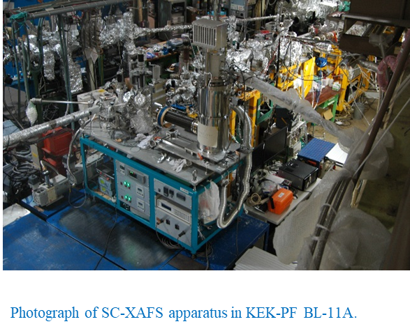
X-ray Absorption Fine Structure Spectroscopy with a Superconducting Fluorescence Detector (SC-XAFS)
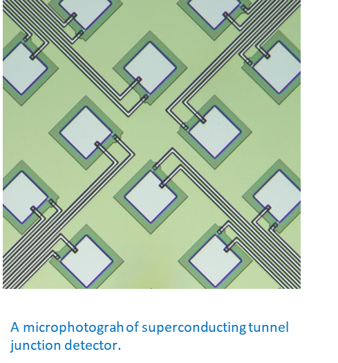
The apparatus provides partial fluorescence yield X-ray absorption spectroscopy using a synchrotron light source and superconducting tunnel junction X-ray spectrometer, achieving an excellent X-ray energy resolution of 10?20eV.1
Applications
・Nanostructures of trace light elements
・K-edge X-ray absorption spectrum of light elements
・L-edge X-ray absorption spectrum of transition metals
・Solid samples(powder, substrate, etc., size less than 15 mm square)
・Infomation about bulk(analysis depth of 100-1000nm)
Principle and Features
・X-ray absorption spectroscopy provides information about nanostructures, such as valence, electronic state, bond length, etc., around a specific element.
・This apparatus measures the X-ray absorption spectrum by measuring the fluorescence yield of a specific element as a function of incident X-ray energy. The electron yield method is generally used to measure the X-ray absorption spectrum in the soft X-ray region, but it is difficult to measure the spectrum of trace elements due to high background. Since the background is small in the fluorescence yield method, even trace elements can be measured. However, in order to obtain the fluorescence yield of trace elements, it is necessary to separate thefluorescence yield of the target element from
the characteristic X-rays of many elements.
By using a superconducting detector with excellent
energy resolution,
it is possible to select elements with high accuracy.
t X-ray beamlines BL-11A, BL-11B, BL-13A,
BL-16A of the Photon Factory of
the High Energy Accelerator Research
Organization can be used as the light source.
xamples
・ Evaluation of SiC characteristics for practical use of high-voltage switch materials
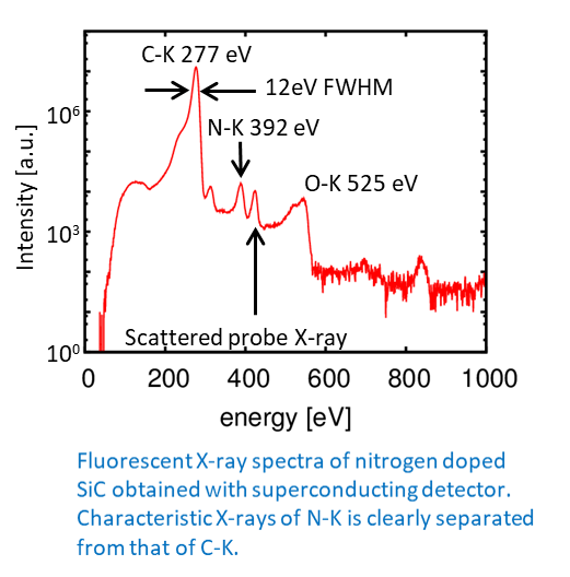
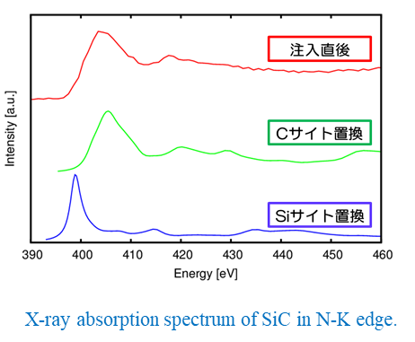
・SiC is a compound semiconductor that is used as a high withstand voltage switch material. Nitrogen is doped into SiC by high-temperature ion implantation. It is necessary to reduce the resistance in order to suppress the power consumption. However, when nitrogen is doped at a high concentration, the activation rate decreases and the resistance value increases. To clarify the location of nitrogen in the lattice after ion implantation and annealing, the fluorescence yield X-ray absorption spectrum at the nitrogen K-edge was measured. Comparison with the simulation revealed that the doped nitrogen was replaced with carbon immediately after ion implantation, and that the structure was not changed by annealing.
・Measurement of GaN to reduce the power consumption of luminescent materials
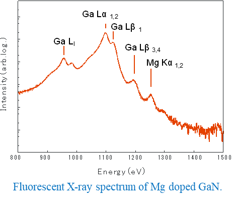
・GaN is a compound semiconductor that is used as a light emitting material. In order to reduce power consumption, it is necessary to increase the activation ratio by doping with Mg etc., but the local structure of the doped Mg cannot be measured due to the interference of the Ga-L line adjacent to the Mg-K line. The fluorescence X-ray spectrum of Mg-doped GaN was measured using the apparatus, and it was found that Ga-L and Mg-K rays could be clearly distinguished. The elimination of Ga-L line interference is expected to help elucidate the local structure of Mg and reduce the power consumption.
Other examples
・Analysis of Na in the solar cell material CIGS
・Analysis of trace elements (S, Cl, etc.) contained in glass
・Effect of chemical state of trace nitrogen on macroporous SiC catalyst activity 3