
Real Surface Probe Microscope(RSPM) RSPM is a nanoprobing system used to characterize nano properties, including electric potential, elastic modulus, and optical response, in various environments (air, liquid or vacuum). It comes with reference materials, cantilever calibrators (spring constant, probe shape), and sample surface preparation devices optimized for scanning probe microscopes (SPM).
Equipment
RSPM 1
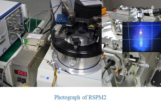
A high-resolution scanning probe microscope, which includes KPFM and nano-manipulation functions.RSPM 2
This scanning probe microscope is used for characterizing nano-materials (KPFM, SNDM, elastic modulus, and spectroscopic images) in various environments such as in air, liquid, and vacuum.Applications
・High-resolution surface morphology measurement with probe calibration system
・Elastic modulus measurement for compliant (DMT or JKR) and stiff materials
・Electrical SPM, such as KPFM, SCM, SNDM, SSRM, and C-AFM
・Fast scanning system in liquids (10 frames/second)
・Surface preparation devices include ion beam polisher, plasma cleaning equipment, laser marking systemPrinciple and Features
・RSPM is a scanning probe microscope with facilities for characterizing nano-materials in various environments such as air, liquid, and vacuum. Fast scanning in liquids is possible. The dynamic mode with laser excitation system produces accurate phase images.
・Reference materials
・Probe shape (probe shank or 3D shape)
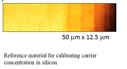
・Reference samples for carrier concentration
・Resolution test sample for various imaging
techniques・Calibration system
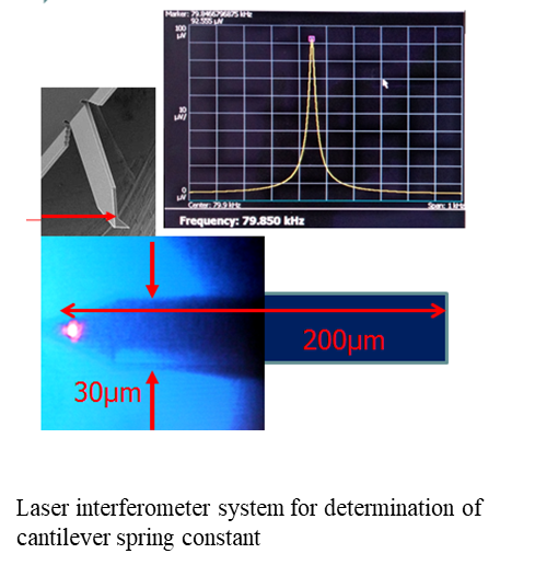
・Laser doppler interferometer for calibrating
normalspring constant of a cantilever
・SEM for probe shape・Sample preparation devices
・Mechanical polishing machine
・Ion milling equipment for preparing cross-sections of thin samples
・Laser marking system for aligning the field of view
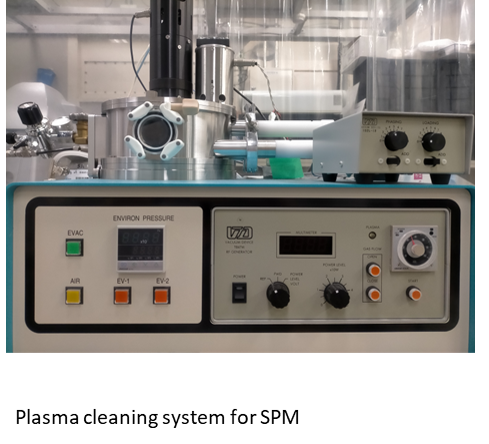
・Plasma surface cleaning system(Ar, O, N)
Examples
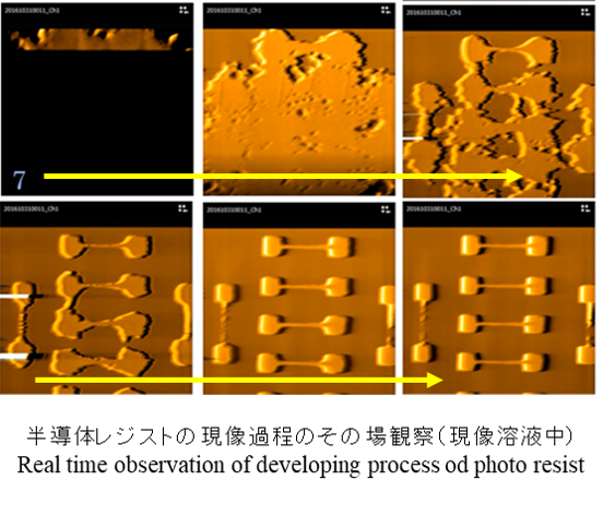
・Developing process of photoresist
・The developing process of photoresist on Si substrate was observed in a liquid. The origin of defects in the electron beam lithography process was studied with a high-speed scanning system. Real-time AFM images were obtained every ten seconds in the developer solution. The photoresist, which is designed as a 50-nm line, was clearly observed as shown in the figures.
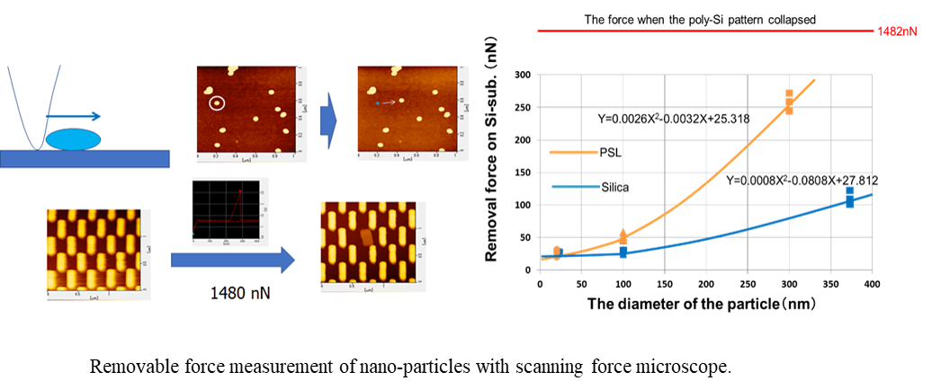
・Removal force of nano-particles on Si substrate
・The removal force of nano-particles on Si substrate was measured with a scanning probe microscope. Forces required to remove particles and nano-patterns were compared. The results will be useful for developing cleaning equipment for semiconductor factories.
Other examples
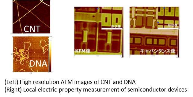
・Surface morphology measurement of nano-
materials such as CNT and DNA
・DNA or large molecules can be observed in
liquid
・Surface potential and carrier concentration in
silicon can be observed with KPFM, SCM and SSRM
・Nano-device measurement in contact mode (current, thermal property) is possible
・High-voltage surface charge can be measured with KPFM
・Nano-devices can be measured while in operation with a device analyzer