Two-Dimensional Materials Nano-Device Team
2D nano material nanodevice team aims developments defect-free/functional transfer processes and doping techniques toward electronic and optics devices of 2D nano material such as graphene and transition metal dichalcogenides (TMDs).
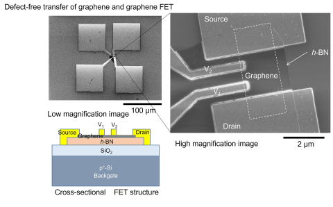
Defect free/functional transfer process
To develop electronic and optics devices of 2D nano materials, it is necessary to transfer to insulator materials. Our team is engaged in the high-quality transfer processes (defects and wrinkles free), and the stacking process of clean interfaces between 2D nano materials and insulator materials.
Doping techniques
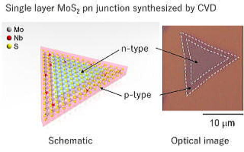
Our team is engaged in doping process to control carrier density and conductivities of 2D nano materials. We are also engaged in expression of new functions by doping, and the evaluation of electrical and optical physical properties.
Team Member
| Position and Name | Specialization | Member Page |
|---|---|---|
Team Leader
Takatoshi Yamada |
Electronic Material, Surface Physical Property, Interfacial Property | |
Senior Researcher
Yuki Okigawa |
Semiconductor Physical Characteristics, Low-Dimensional Material Electronics | |
|
Senior Researcher
Takeshi Fujii |
Thin film growth, Semiconductor device bonding | |
Senior Researcher
Mitsuhiro Okada |
Crystal Growth, Semiconductor Properties | |