研究紹介

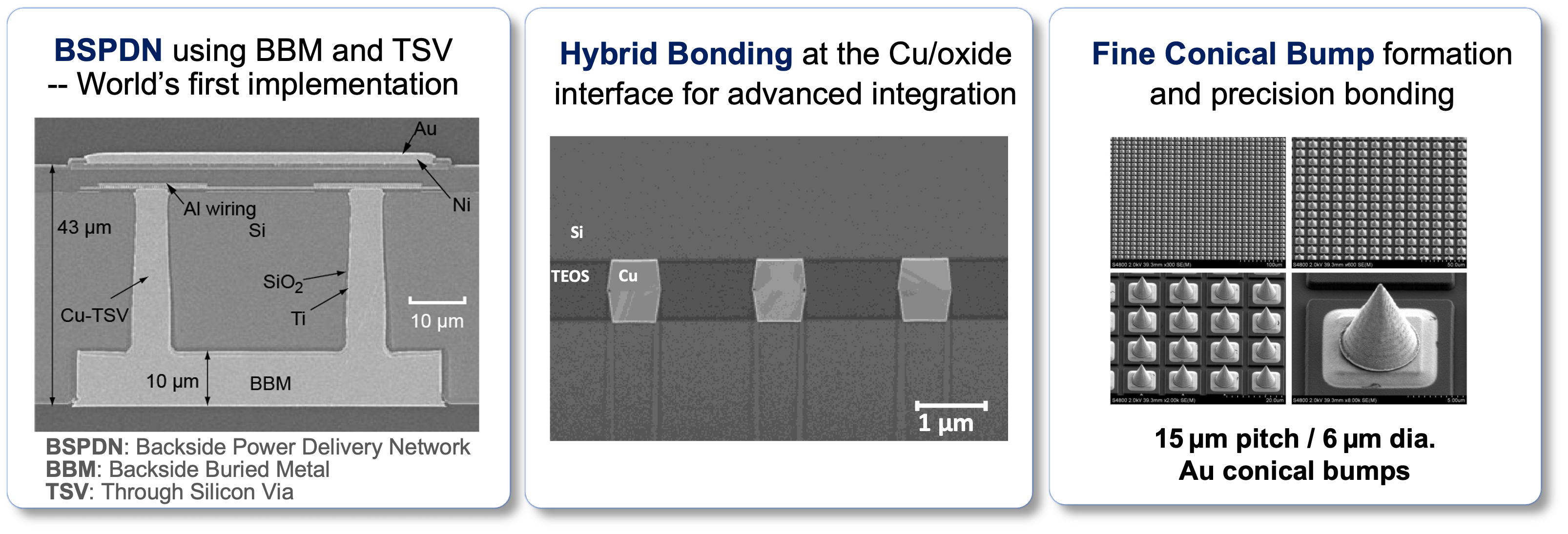
3D Integration
- 3D Integration and Packaging
- HDevelopment of key technologies for high-density 3D integration, leveraging seamless process integration across front-end, mid-end, and back-end.
- System-Level Design and Evaluation
- R&D on system-level design, simulation, and evaluation technologies to maximize the potential of 3D integration.
- FPrototyping Hub for 3D Integration
- Establishing a prototyping hub equipped with 3D integration and semiconductor tools, aiming for a full-stack development environment..
MEMS / Wafer Bonding / Sensing / Packaging
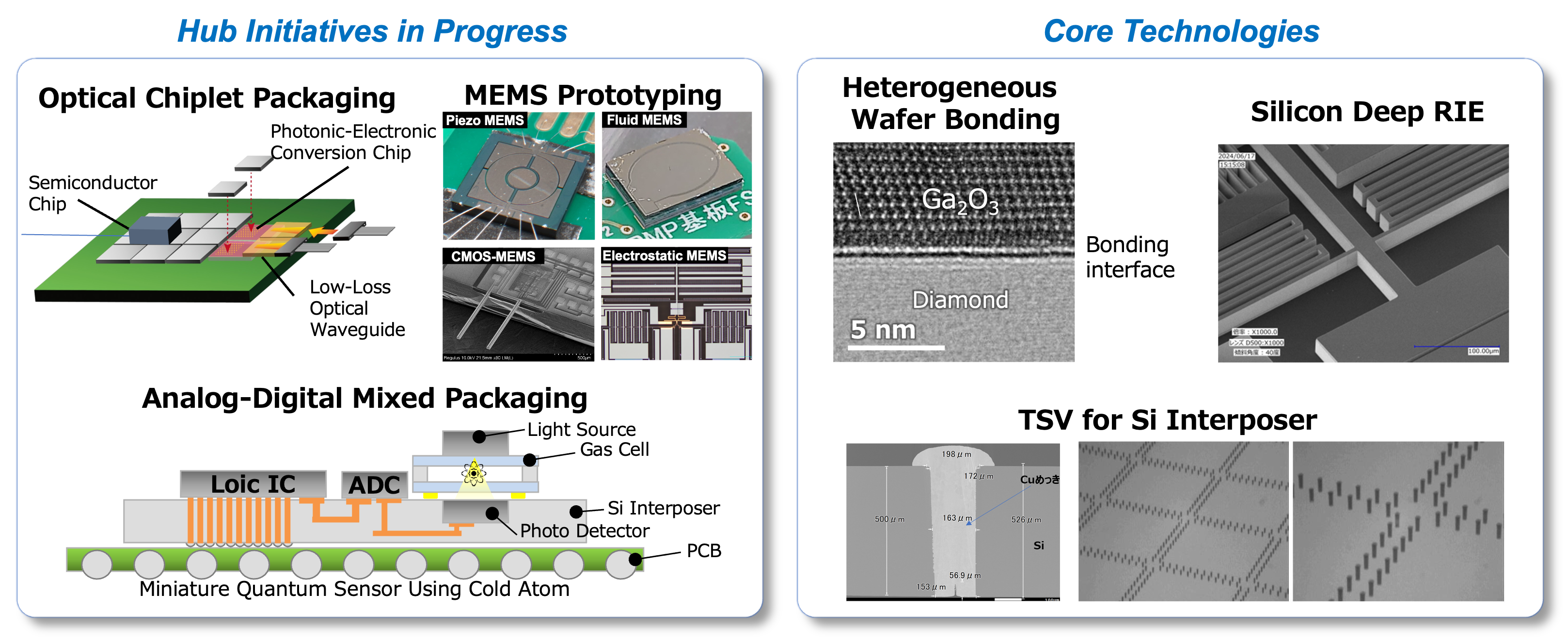
- Advanced Packaging and Assembly Technologies
- Hybrid packaging built upon MEMS prototyping. Key strengths: advanced silicon deep RIE, glass processing, heterogeneous wafer bonding.
- 3Comprehensive Backend Process Hub
- Integration with the 3D Integrated System Development Hub. Advancing packaging technologies and fostering talent. Toward a central base for advanced packaging processes.
Spintronics / Quantum Tech
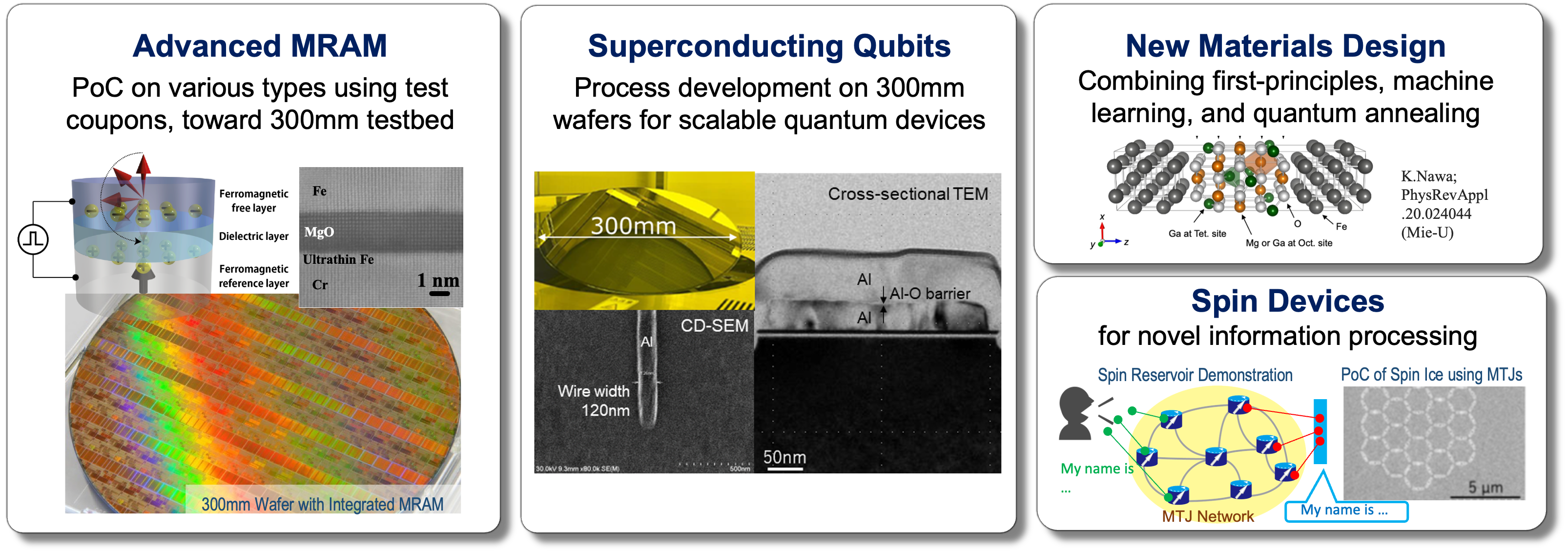
- Next-Generation MRAM Development
- High-speed, ultra-low-power, and reliable nonvolatile memory for cache, main memory, and storage-class applications. Examples include VC-MRAM, SOT-MRAM, and cross-point STT-MRAM.
- 300mm-Scale Quantum Process Platforms
- Large-scale fabrication of superconducting circuits for quantum computing based at the Super Clean Room (SCR), AIST’s advanced 300mm process platform.
- Fundamental Science and Materials for the Next Paradigm
- Brain-inspired computing by spintronics memories and oscillators for information processing, Highly sensitive magnetic sensor, and First-principles investigation of new magnetic materials.