Uptake and accumulation mechanisms of hexachloroplatinate(IV) ions in the unicellular alga, Pseudococcomyxa simplex (Metallomics)
|
Platinum uptake was examined by adding hexachloroplatinate(IV) solution to the unicellular alga Pseudococcomyxa simplex. After the addition of platinum solution ([Pt] = 100 mg/kg, pH 3.2–3.4) for a certain time, the cells were quickly frozen and subjected to μ-XRF (X-ray fluorescence) analysis using synchrotron X-rays. The beam size of approximately 1 micrometer allowed visualization of the platinum distribution within a single cell. On the other hand, we examined platinum uptake in enzyme-treated protoplasts and lyophilized cells and found that the platinum uptake concentrations in these samples were higher than in living in-vivo cells. Cell wall and cell metabolism were presumed to interfere with the uptake of hexachloroplatinate(IV) ions. All platinum ions taken up by the cells were reduced to divalent form. The effect of light on platinum addition was also investigated. When platinum was added under light conditions, some samples showed higher platinum accumulation than under shade conditions.
Link |
Evaluation of the change in photoresist sidewall roughness due to electron beam-induced shrinkage using atomic force microscopy (J. of Micro/Nanopatterning, Materials, and Metrology)
|
Background: Scanning electron microscopy (SEM) is commonly employed for line edge roughness (LER) measurements; however, achieving high-precision LER measurement of photoresists is difficult through this approach because electron beam (EB) exposure causes shrinkage of materials. Moreover, the differences in the 3D sidewall shape before and after shrinkage have not been investigated in detail. Aim: Evaluation of the impact of photoresist shrinkage induced by EB exposure on the sidewall roughness of a pattern. Approach: The shrinkage was observed by measuring a photoresist pattern before and after EB exposure using atomic force microscopy with a tip-tilting technique (tilting-AFM). Results: EB exposure smoothed the surface roughness, rounded the top corners, and reduced the pattern height. Roughness parameters evaluated via LER analysis showed that with shrinkage, the standard deviation (σ) and roughness exponent (α) decreased, while the correlation length (ξ) increased. Conclusions: The results show that SEM-based LER measurements may lead to underestimation of σ and α, and the overestimation of ξ because of the effect of EB-induced shrinkage. Overall, we establish a tilting-AFM technique to evaluate the 3D shape of photoresist patterns without EB damage and with high resolution and low noise. Link |
Experimental evaluation of usable specimen thickness of Si for lattice imaging by transmission electron microscopy at 300 kV (Ultramicroscopy)
|
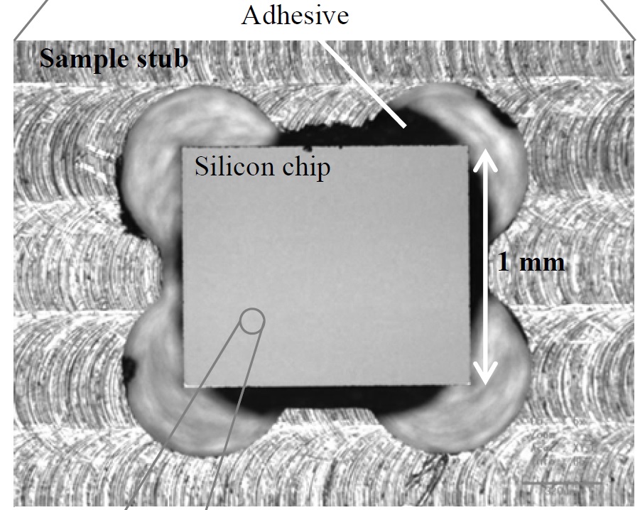
We evaluated the usable specimen thickness of Si for lattice imaging on a transmission electron microscopy (TEM) instrument operating at 300 kV and equipped with a complementary metal-oxide-semiconductor camera by using an original reference material (RM) and comparing the lattice images obtained from Si patterns of the RM with various thicknesses. Lattice images of the {111} planes of crystalline Si are successfully observed for patterns with thicknesses of up to 508 nm. However, the contrast of these lattice fringes at a thickness of 508 nm is not distinct, even when recorded using a longer exposure time (5.0 s) than that required to obtain lattice images of patterns with thicknesses of 316 nm or less (0.5 s). Based on these results, we conclude that the practical thickness of crystalline Si specimens for accurate structural analysis and TEM magnification calibration via lattice imaging is less than approximately 500 nm under the experimental conditions.
Link |
Contrast mechanism at landing energy near 0 eV in super low-energy scanning electron microscopy (Microscopy)
|
In recent years, the technique of scanning electron microscopy (SEM) observation with low landing energy of a few keV or less has become common. We have especially focused on the drastic contrast change at near 0 eV. Using a patterned sample consisting of Si, Ni and Pt, threshold energies where the total reflection of incident electrons occurs were investigated by SEM at near 0 eV. In both the cases of in-situ and ex-situ sample cleaning, drastic changes in the brightness of each material were observed at near 0 eV, with threshold energies in the order Si < Ni < Pt. This order agreed with the order of the literature values of the work functions and the surface potentials measured by Kelvin force probe microscopy. This result suggests that the difference of the threshold energy is caused by the difference in surface potential due to the work function difference of each material. Although the order of the threshold energies also agreed with those of work functions reported in the literature, the work functions of air-exposed surfaces should be rather considered as ‘modified work functions’, since they could be significantly altered by the adsorbates, etc. Nevertheless, the difference of the threshold energy for each material was observed with commercial SEM at landing energy near 0 eV, which opens a new possibility to distinguish materials, although the difference should be rather recognized as ‘fingerprints’, since surface potentials are sensitive to conditions of surface treatments and atmospheric exposure.
Link |
Effect of white noise on roughness measurements of self-affine fractals (Measurement Science and Technology)
|
This study formulated and clarified the presentation of the noise-related error terms in the power spectral density (PSD) and height–height correlation function (HHCF) through a roughness analysis of self-affine fractals. Assuming the noise as white noise, this study simulated the PSD and HHCF of the noisy roughness profile in a typical situation: line-edge roughness measurements involved in semiconductor lithography technology. It was found that conventional noise-correction techniques can bias the PSD/HHCF from those of the true roughness profiles because they do not account for the residual noise-induced error. The findings obtained from the roughness analysis and simulation techniques are expected to benefit various applications, such as clarifying the quantitative residual error in specific situations, selecting the optimum analysis method (PSD or HHCF), estimating the required number of averaged profiles (measurements) that yields sufficiently small noise errors, and considering strategies for noise reduction.
Link |
Developmental framework of line edge roughness reference standards for next-generation functional micro-/nanostructures (Precision Engineering)
|
The edge of a micro-/nanoscale line pattern fabricated by lithography is not a straight line as in the design but has a roughness. This is called the line edge roughness (LER) and is important dimensional information related to the device performance, and reference standards containing known LER values are needed for fundamental research on lithography-related technology. We propose a novel framework for developing LER reference standards that contain the necessary characteristics. The proposed framework has three main features: (i) a self-affine fractal roughness model for the development of next-generation devices; (ii) a reliable evaluation method based on LER reference metrology using SI-traceable atomic force microscopy (AFM); and (iii) a versatile evaluation method using scanning electron microscopy-based LER metrology verified by the previous AFM-based LER reference metrology. In an experiment to verify the proposed framework, we fabricated an LER reference standard by using electron-beam lithography. The results show that the proposed framework can be used to develop LER reference standards for next-generation functional micro-/nanostructures.
Link |
Photoresist shrinkage observation by a metrological tilting-AFM (Proc. SPIE)
|
Scanning electron microscopy (SEM) is commonly used for line edge roughness (LER) measurement; however, it is difficult to achieve high-precision LER measurement of photoresists because exposure to an electron beam (EB) causes shrinkage of the materials. The differences in the 3D sidewall shape before and after shrinkage have not been investigated in detail. In this study, EB-induced photoresist shrinkage was observed by employing the atomic force microscopy with tip-tilting technique (tilting-AFM), which enables high-precision observation of the vertical sidewall of the pattern. In the experiment, the shrinkage deformation was observed by measuring the same photoresist pattern with the tilting-AFM before and after EB exposure (by SEM observation) on the pattern. The results show that the sidewall was smoothed by EB exposure. Further, the tendency of changes in LER (roughness parameters) was observed. This measurement technique can be used to better understand photoresist materials and to improve the LER measurement by SEM.
Link |
Tellurium Nanorods Produced by the Reduction of Tellurate and Tellurite Inside Unicellular Algae (Chemistry Letters)
|
The addition of oxoanions of tellurium to unicellular alga, Pseudocococcomyxa simplex, resulted in a high accumulation of tellurium. Tellurium was reduced during cellular uptake and nanorods of metallic tellurium (200-600 nm) were formed inside the cells. Electron microscopy of cells without any chemical pretreatment allowed direct observation of the presence of intracellular tellurium nanorods.
Link |
Enhancing the precision of 3D sidewall measurements of photoresist using atomic force microscopy with a tip-tilting technique (Journal of Applied Physics)
|
A key issue associated with advanced lithography techniques for semiconductor-device manufacturing is the reduction in the sidewall roughness of photoresist line patterns, known as line-edge roughness (LER). We have developed a technique for measuring the sidewall of the resist pattern using atomic force microscopy (AFM) that enables three-dimensional (3D), high-resolution, low-noise, and nondestructive measurements. Conventional LER measurement technology using scanning electron microscopy (SEM) causes shrinkage of the resist pattern due to electron-beam (EB) exposure, whereas our new AFM technique can in principle avoid EB-induced shrinkage. This AFM technology is capable of 3D measurements because it employs a tip-tilting mechanism that enables the sharp AFM tip to scan the vertical sidewalls, which is difficult for a conventional AFM technique. In addition, laser interferometers are equipped for the measurement of the AFM tip displacement, which yields high-resolution, high-accuracy, and low-noise results. This technology overcomes issues such as low resolution, noise, and destructive measurements that afflict conventional SEM measurements. In addition, it enables observations and quantitative analyses of the 3D sidewall roughness. For example, in the present experiment, we observed that grain shapes (several tens of nm in size) were formed randomly on the resist sidewall and that there were almost no footing shapes. By analyzing the sidewall profiles with a height resolution of 1 nm, we obtain the roughness (self-affine fractal) parameters at each height. This AFM-based resist sidewall measurement technique can, thus, provide important insights into resist patterning and related process technologies for next-generation semiconductor-device manufacturing.
Link |
Pitch calibration of standard nanoscale for uncertainty reduction of certified reference materials for SEM image sharpness evaluation and magnification calibration (Surface Topography: Metrology and Properties)
|
Scanning electron microscopy (SEM) is widely used to observe and analyze nanostructures on surfaces. To obtain accurate and sharp images by SEM, it is necessary to evaluate the sharpness of SEM images and calibrate the magnification simultaneously. The NMIJ-CRM 5207-a is a certified reference material for image sharpness evaluation and magnification calibration. The certified values of NMIJ-CRM 5207-a are the average pitches in the X- and Y- axes. The major source of uncertainty of the NMIJ-CRM 5207-a is the pitch calibration of the commercially available standard nanoscale. To reduce the uncertainty of the pitch calibration value of the standard nanoscale, the pitch calibration was performed using a metrological atomic force microscope and uncertainty was evaluated in this study.
Link |
Formation of biogenic tellurium nanorods in unicellular green alga Chlamydomonas reinhardtii (Metallomics)
|
Tellurium (Te) is an industrially useful element but causes environmental contamination. The formation of biogenic Te nanorods (Te-BgNRs) in plants is one of the Te detoxification pathways associated with the phytoremediation of Te because Te-BgNRs contain low-toxicity Te at high densities. In this study, we investigated the mechanism of Te-BgNR formation in a common unicellular green alga, Chlamydomonas reinhardtii. Electron microscopic observations revealed that the insoluble Te was rod-shaped elemental Te, i.e., Te-BgNRs, and had a highly crystalline nanostructure. These findings suggest that the algal cells initially metabolized tellurate to form soluble Te compounds, and excess tellurate that could not be metabolized was then transformed to Te-BgNRs, which are less toxic than tellurate. Our findings provide a novel approach to Te remediation through the formation of BgNRs in C. reinhardtii.
Link |
Unbiased line edge roughness measurement using profile-averaging method for precise roughness parameters measurement (J. of Micro/Nanopatterning, Materials, and Metrology)
|
Background: Scanning electron microscopy (SEM)-based line edge roughness (LER) measurement suffers from an error due to noise in SEM image. Noise correction methods have been developed to obtain unbiased roughness results, however, there are still concerns in the viewpoint of measurement precision. Aim: To develop an unbiased roughness analysis for highly precise LER measurement. Approach: Combining the conventional unbiased roughness analysis with a profile-averaging method, where a line pattern is repeatedly measured and then the obtained profiles are aligned and averaged. The experimental result measured by SEM was verified using atomic force microscopy (AFM)-based LER metrology, which has higher reliability than SEM. Results: The experimental evaluation showed that the proposed method can obtain roughness parameters more precisely than the conventional method. Conclusions: When the noise in the line edge profile by SEM is too large, it is necessary to reduce the noise beforehand and then perform roughness analysis in order to obtain precise roughness results. The proposed method enables to measure LER with the highest precision using SEM. Additionally, the AFM-based LER metrology was demonstrated as a feasible technique to evaluate the performance of SEM-based LER metrology. Link |
Effect of specimen processing for transmission electron microscopy on lattice spacing variation in Si specimens (Ultramicroscopy)
|
Variation in the (220) lattice spacing of Si due to specimen processing for transmission electron microscopy (TEM) was experimentally evaluated by comparing the measured lattice spacings of crystalline specimens processed by crushing, mechanical polishing only, and combined mechanical and Ar ion polishing. Although distinct variation in the (220) lattice spacing between the Si specimens processed by crushing and by mechanical polishing only is not observed, the (220) lattice spacing of specimens prepared by combined mechanical and Ar ion polishing imply increasing tendency with increasing Ar ion beam irradiation time. Moreover, the (220) lattice spacing measured from the outermost region of the specimen edge tends to be approximately 3% to 5% larger than that measured from the inner region, irrespective of the processing method. These results demonstrate that differences in the processing conditions of Si specimens and in the measurement location of the Si lattice spacing can be major component of the measurement uncertainty in sub-nanometer metrology using TEM with magnification calibration by the Si lattice spacing. When attempting to apply the lattice spacing of Si as a reference with traceability to the International System of Units for TEM magnification calibration in sub-nanometer metrology, the results suggest that the effect of specimen processing on variation in the lattice spacing is not negligible.
Link |
Application of NMIJ CRM 5207-a Tungsten Dot-array:
Reliable Evaluation of the Lateral Resolution of a Confocal Raman Microscope by Using the Tungsten-dot Array Certified Reference Material (Analytical Sciences)
|
Confocal Raman microscopes are widely used in various applications because they provide physical and chemical information at a submicron scale. A high lateral resolution in the confocal Raman microscope is essential for obtaining high-quality images. We used an array of tungsten dots at a 600 nm pitch on a Si substrate of the certified reference material (NMIJ CRM 5207-a) to reliably evaluate the lateral resolution of a confocal Raman microscope at various pinhole sizes. The precision of the mapping scale in the x- and y-pitches was confirmed from Si signal profiles, and the lateral resolution was evaluated by a straight-edge method using scale indicators in the reference material. Because these procedures are applicable to other confocal Raman microscopes with popular specifications (532 nm laser, 100× objective lens, numerical aperture 0.9, step size 0.1 μm), they are suitable for both a reliable evaluation of the lateral resolution of a confocal Raman microscope and for daily checks on the precision of its mapping scale.
Link |
Formation Mechanism and Toxicological Significance of Biogenic Mercury Selenide Nanoparticles in Human Hepatoma HepG2 Cells (Chem. Res. Toxicol.)
|
It is widely recognized that the toxicity of mercury (Hg) is attenuated by the simultaneous administration of selenium (Se) compounds in various organisms. In this study, we revealed the mechanisms underlying the antagonistic effect of sodium selenite (Na2SeO3) on inorganic Hg (Hg2+) toxicity in human hepatoma HepG2 cells. Observations by transmission electron microscopy indicated that HgSe (tiemannite) granules of up to 100 nm in diameter were accumulated in lysosomal-like structures in the cells. The HgSe granules were composed of a number of HgSe nanoparticles, each measuring less than 10 nm in diameter. No accumulation of HgSe nanoparticles in lysosomes was observed in the cells exposed to chemically synthesized HgSe nanoparticles. This suggests that intracellular HgSe nanoparticles were biologically generated from Na2SeO3 and Hg2+ ions transported into the cells and were not derived from HgSe nanoparticles formed in the extracellular fluid. Approximately 85% of biogenic HgSe remained in the cells at 72 h post culturing, indicating that biogenic HgSe was hardly excreted from the cells. Moreover, the cytotoxicity of Hg2+ was ameliorated by the simultaneous exposure to Na2SeO3 even before the formation of insoluble HgSe nanoparticles. Our data confirmed for the first time that HepG2 cells can circumvent the toxicity of Hg2+ through the direct interaction of Hg2+ with a reduced form of Se (selenide) to form HgSe nanoparticles via a Hg–Se soluble complex in the cells. Biogenic HgSe nanoparticles are considered the ultimate metabolite in the Hg detoxification process.
Link |
Research Activities of Nanodimensional Standards Using Atomic Force Microscopes, Transmission Electron Microscope, and Scanning Electron Microscope at the National Metrology Institute of Japan (Nanomanufacturing and Metrology)
|
With the progress in nanotechnology, the importance of nanodimensional standards is increasing. Realizing nanodimensional standards requires multiple types of high-precision microscopy techniques. The National Metrology Institute of Japan (NMIJ), one of the research domains in the National Institute of Advanced Industrial Science and Technology (AIST), is developing nanodimensional standards using atomic force, transmission electron, and scanning electron microscopes. The current status of nanodimensional standards in NMIJ is introduced herein.
Link |
Extension of the probe-tip error evaluation for areal surface roughness measurements using metrological AFM (Measurement: Sensors)
|
Recently, there have been increasing demands not only for the conventional profile surface roughness measurements using atomic force microscopes (AFM) but also for areal surface roughness measurements. In this study, a technique using one of the areal surface roughness parameters is proposed in order to extend the conventional method of profile roughness measurements specified in ISO 19606:2017 to areal roughness measurements.
Link |
Chromogenic Amorphous MoO3–x Nanosheets and Their Nanostructured Films for Smart Window Applications (ACS Applied Nano Materials)
|
Amorphous molybdenum trioxide (a-MoO3–x) nanosheets of approximately 1.5 nm thickness were synthesized via pseudo-topotactic reactions of two-dimensional MoO2 nanosheets obtained soft-chemically from the exfoliation of layered sodium molybdate, Na0.9Mo2O4. The topotactic phase transformation from the as-grown MoO2 nanosheets to crystalline MoO3–x nanosheets was triggered by a facile calcination at 200 °C in air. Amorphization without significant changes in the sheet structure occurred at 250 °C, yielding a-MoO3–x nanosheets. Among the products, a monolayer film of the a-MoO3–x nanosheets had superior photochromic properties in the visible and infrared ranges via band-gap excitation compared to conventional thin films composed of MoO3-related materials in terms of coloration efficiency, that is, degree of coloration per thickness. The coloration efficiency of the a-MoO3–x nanostructured films fabricated in this study remained unchanged despite an increase in the stacking number of the precursor nanosheets because the amorphous structure inhibited the recombination of electron–hole pairs; moreover, the multilayer structure had interlayer galleries between the nanosheets. Consequently, the thick film comprising layers with a similar a-MoO3–x nanostructure exhibited a remarkable degree of coloration and repeatability of coloration and bleaching cycles, indicating its potential for smart window applications.
Link |
Experimental evaluation of uncertainty in sub-nanometer metrology using transmission electron microscopy due to magnification variation (Measurement Science and Technology)
|
Uncertainties due to the magnification variation in sub-nanometer metrology using transmission electron microscopy (TEM) were experimentally evaluated by comparing the measured values of the (220) lattice spacing of a crystalline Si specimen acquired under various conditions. Interday variation of the magnification, intraday repeatability, rotation of the TEM image, specimen exchange, specimen position, defocusing, magnetic hysteresis of the lenses, projection lens distortion, and measurement errors were considered as the uncertainty components. The obtained results reveal that the major uncertainty components are the interday magnification variation, intraday repeatability involving nonuniformity of the specimen structure, magnetic hysteresis of the intermediate lenses, and projection lens distortion. Among these components, it is expected to be feasible to suppress the interday magnification variation to a negligible level by daily magnification calibration, suggesting that minimizing the uncertainties due to magnetic hysteresis of the intermediate lenses, projection lens distortion, and nonuniformity of the specimen structure will be the key factor for further reducing the uncertainty of sub-nanometer metrology using TEM. Furthermore, we found that magnification calibration using an appropriate reference material (e.g., the lattice fringes of crystalline Si) before every measurement should enables sub-nanometer metrology with a relative uncertainty of 3.2%, even if the specimen is introduced into the TEM system by specimen exchange after magnification calibration.
Link |
Nanoscale Standards by Metrological AFM and Other Instruments (IOP ebooks)
 |
The purpose of this book is to help semiconductor inspection equipment users and manufacturers understand what nano dimensional standards are used to calibrate their equipment and how to employ them effectively. Reviewing trends and developments in nanoscale standards, the book starts with an introductory overview of nanometrological standards before proceeding to detail pitch standard, step height, line width, nano particle size, and surface roughness. This book is essential for users making quantitative nanoscale measurements, be that in a commercial or academic research setting, or involved in engineering nanometrology for quality control in industrial applications. Here the author provides an approachable understanding and application of the nanoscale standards in a practical context across a range of common nanoscale measurement modalities, including 3D, with particular emphasis on applications to AFM, an exceptional and arguably the most common technique used in nanometrology due to the ease of use and versatility of applications.
Link |
Evaluating SEM-based LER metrology using a metrological tilting-AFM (SPIE Proceedings)
|
In this study, we developed a methodology to evaluate scanning electron microscopy (SEM)-based line edge roughness (LER) metrology. In particular, we used a metrological tilting atomic force microscopy (tilting-mAFM) as LER reference metrology. We analyzed the height-height correlation function (HHCF) of SEM line-edge profiles combining averaging and unbiased correction methods. The direct comparison of our method with tilting-mAFM enabled a precise evaluation of the SEM-based LER metrology. We demonstrated that a combination of unbiased HHCF and averaging methods with appropriate condition enabled relatively precise measurement of three roughness parameters. We observed that, for precise roughness evaluation, reducing noise in the line-edge profiles is important before performing the HHCF analysis and unbiased correction.
Link |
Evaluation of Image Distortion in Sem by Using a Dot-Array Based Certified Reference Material (Microscopy)
|
This paper presents a quick and straightforward method to evaluate image distortion in scanning electron microscopy (SEM) using a certified reference material (CRM) as a test specimen. The CRM has a square dot-array structure, whose dot-pitch has an accredited value. By calculating the distance between each dot of the CRM via image analysis, we can detect the distortion in the image as variations of dot interval. Furthermore, by considering the uncertainty of the certified value, it is possible to quantitatively evaluate the significance of the distortion in the image. This method enables us to easily estimate the uncertainty from image distortion, which can improve the reliability of measurement by SEM.
Link |
Direct comparison of line edge roughness measurements by SEM and a metrological tilting-atomic force microscopy for reference metrology (J. of Micro/Nanolithography, MEMS, and MOEMS)
|
Background: Conventional scanning electron microscopy (SEM) that is used for 2D top-view metrology, a classical line edge roughness (LER) measurement technique, is incapable of measuring 3D structures of a nanoscale line pattern. For LER measurements, SEM measurement generates a single line-edge profile for the 3D sidewall roughness, although the line-edge profile differs at each height in the 3D sidewall. Aim: To develop an evaluation method of SEM-based LER measurement techniques and to verify how the 3D sidewall shape is reflected in the SEM’s 2D result. Approach: Direct comparison by measuring an identical location of a line pattern by SEM and an atomic force microscopy (AFM) with the tip-tilting technique that is capable of measuring the 3D sidewall. The line pattern has vertical stripes on the sidewall due to its fabrication process. Measured line edge profiles were analyzed using power spectral density, height-height correlation function, and autocorrelation function. Results: Line edge profiles measured by SEM and AFM were well matched except for noise level. Frequency and scaling analyses showed that SEM profile contained high noise and had lost a property of self-affine fractals in contrast to AFM. Conclusions: In the case of the line pattern with vertical stripes on the sidewall, SEM profile is generally consistent with 3D sidewall shape. The AFM-based LER measurement technique is useful as LER reference metrology to evaluate other LER measurement techniques. Link |
Development of NMIJ CRM 5207-a tungsten dot-array for the image sharpness evaluation in scanning electron microscopy – structure evaluation and determination of dot-pitch (Microscopy)
|
We have developed a new certified reference material (CRM) for image sharpness evaluation and magnification calibration for scanning electron microscopy (SEM). Designed to be suitable for the image sharpness evaluation by the derivative method, the CRM has nanoscale tungsten dot-array structure fabricated on silicon substrate, which gives steep contrast transition from the dot to the substrate in SEM image. The pitch of the dot-array was SI-traceably measured as a specified value with relative expanded uncertainty of ~1.3%, which can be utilized for the magnification calibration of SEM. Since specimens, as one of the image formation parameters, easily affect image sharpness value, our CRM, as a ‘pinned specimen’, will play an important role to achieve robust and stable image sharpness measurement system.
Link |
Elucidation of tellurium biogenic nanoparticles in garlic, Allium sativum, by inductively coupled plasma-mass spectrometry (Journal of Trace Elements in Medicine and Biology)
|
Although tellurium (Te) is a non-essential, non-beneficial, and toxic element in living organisms, it is reported that garlic (Allium sativum) can accumulate Te by assimilation to produce organotellurium compounds including telluroamino acids. In this study, we revealed a novel Te metabolic pathway for the formation of insoluble Te nanoparticles in garlic. Because Te biogenic nanoparticles are non-toxic to organisms, their formation could be an important metabolic pathway for the detoxification of inorganic Te as well as the synthesis of organotellurium compounds. In addition, garlic can be successfully applied to the phytoremediation of Te in the environment.
Link |
A standard used for probe-tip diameter evaluation in surface roughness measurements using metrological atomic force microscope (Measurement Science and Technology)
|
Recently metrological atomic force microscopes (metrological AFMs) have been used for surface roughness measurements. The National Metrology Institute of Japan (NMIJ), AIST, provides a profile surface roughness calibration service using a metrological AFM based on ISO 19606:2017. This international standard requires evaluation of probe-tip diameter D and error in roughness measurements by using a standard plate with needle-shaped spikes before conducting surface roughness measurements. However, the conventional standard plate has several problems: (1) needle-shaped spikes are too high, (2) the distance between spikes is too long, and (3) spike curvature radius is not small enough, compared with AFM probe-tip size, which may lead to considerable uncertainty derived from probe-tip error evaluation. This study examined a new type of commercially-available standard plate as a candidate for probe-tip diameter evaluation. It features lower spike height and shorter distance between spikes in order to avoid probe-tip wear caused by repeated scanning. This study demonstrated that the overestimated uncertainty derived from probe-tip error evaluation can be corrected by using the new standard plate.
Link |
Line edge roughness measurement on vertical sidewall for reference metrology using a metrological tilting atomic force microscope (J. of Micro/Nanolithography, MEMS, and MOEMS)
|
Line edge roughness (LER) measurement is one of the metrology challenges for three-dimensional device structures, and LER reference metrology is important for reliable LER measurements. For the purpose of LER reference metrology, we developed an LER measurement technique that can analyze LER distribution along the height of a line pattern, with high resolution and repeatability. A high-resolution atomic force microscopy (AFM) image of a vertical sidewall of a line pattern was obtained using a metrological tilting-AFM, which offers SI-traceable dimensional measurements. The tilting-tip was controlled with an inclined servo axis, and it scans the vertical sidewall along a line pattern with a high sampling density to enable an analysis of the LER height distribution at the sidewall. A horizontal cross-section of the sidewall shows sidewall roughness with sub-nm resolution. Power spectral density (PSD) analysis of the sidewall profile showed that the PSD noise in the high-frequency region was several orders of magnitude lower than the noise of typical scanning electron microscopy methods. AFM measurements were sequentially repeated three times to evaluate the repeatability of the LER measurement; results indicated a high repeatability of 0.07 nm evaluated as a standard deviation of LER at each height.
Link |
A reference-scan-based method for correcting the nonlinear drift of atomic force microscopy at sub-nanometer precision (Measurement Science and Technology)
|
A known fundamental issue with atomic force microscopy (AFM) is that drift occurs during an AFM measurement, distorting the AFM image. In this study, a method for correcting this nonlinear drift in two dimensions (the vertical axis and one of the two horizontal axes) is proposed and demonstrated. A normal AFM measurement is accomplished with many fast-scan profiles, using the raster scan method. In the proposed drift-correction method, the first-scanned profile is set as the reference profile, and the scan at the first-scanned location is inserted periodically during the normal profile scans. The normal scanned profiles are used to construct a normal AFM image, which is distorted by the drift. The time-dependent drift distance can be estimated by a series of the scanned reference profiles, and the distorted AFM image is corrected using this estimated distance. It is shown, experimentally, that the drift correction in two dimensions has both high resolution and repeatability at the sub-nanometer scale.
Link |
Nanoparticle Characterization - Supplementary Comparison on Nanoparticle Size (Metrologia)
|
Nanoparticles with size in the range from 10 nm to 300 nm and from three different materials (Au 10 nm, Ag 20 nm, and PSL 30 nm, 100 nm and 300 nm) were used in this supplementary comparison. The selected nanoparticles meet the requirements of different measurement methods such as Atomic Force Microscopy (AFM), Transmission Electron Microscopy (TEM), Scanning Electron Microscopy (SEM), Dynamic Light Scattering (DLS), and Differential Mobility Analyzer (DMA), Small Angle X-Ray Scattering and for forth.
Link |
Traceable Atomic Force Microscope for Surface Roughness Calibration of Sub-Nanometer Order —An Overview of The LST-AFM and Its Temperature Stability— (Journal of the Japan Society for Precision Engineering)
|
Calibration technology of profile surface roughness (Ra: from 0.2 nm to 100 nm) by using an atomic force microscope with differential laser interferometers (DLI-AFM) has been developed at NMIJ, AIST. Recently, there have been increasing needs for calibration service of surface roughness of sub-nanometer order. In order to realize surface roughness calibration of sub-nanometer order using the DLI-AFM, however, several challenges remain unaddressed, including scanning stability and drift. At present, authors are developing a length-standard-traceable AFM (LST-AFM) to calibrate surface roughness calibration of sub-nanometer order with a small uncertainty. In this LST-AFM, a reference mirror for the z-axis interferometer is mounted on the AFM cantilever probe unit so as to realize more stable surface roughness calibration. An overview of the LST-AFM, stability of temperature and a light source of an AFM optical lever system are reported in this paper.
Link |
Measurement of the number concentration of gold nanoparticle suspension by scanning electron microscopy (Metrologia)
|
Measuring the number concentration (NC) of nanoparticles (NPs) in suspension has become important because of its use as an index of the quality and efficacy of medical and industrial products. Although scanning electron microscopy (SEM) can reveal individual particles, it is not commonly used for measurement owing to difficulties in sample preparation. We used a micro-liquid dispenser to prepare a specimen of a gold NP suspension, and by combining SEM and gravimetry we measured the NC. The dispenser places a small droplet of suspension onto a Si substrate without splashing, confining the particles in a small area. This method enabled us to observe and count all particles in the area by SEM without loss. The average weight of droplets was determined from weight increments of multiple ejections from the dispenser into a reservoir on an analytical balance. Dividing the NP number by single droplet weight gives NC in g−1. Our simple method gave a precise measurement of the NC of Au NPs with a relative expanded uncertainty of <6% (k = 2) by identifying all particles in a droplet.
Link |
Extension of the range of profile surface roughness measurements using metrological atomic force microscope (Precision Engineering)
|
The calibration of surface roughness by using a metrological AFM has been operated. The calibration range of Ra is now extended. It is in the range of about 0.2 nm–100 nm. The range satisfies the demand from precision machining and semiconductor industries.
Link |
Linewidth calibration using a metrological atomic force microscope with a tip-tilting mechanism (Measurement Science and Technology)
|
The linewidth or critical dimension (CD) of a nanoscale line pattern is calibrated using a metrological atomic force microscope with a tip-tilting mechanism (tilting-mAFM). The tilting tip allows scanning of the line pattern's vertical sidewalls. The tilting-mAFM performs two measurements on each side of the line pattern, and two datasets are stitched together to reconstruct the complete shape of the line pattern. Further, CD is measured based on this pattern. A linewidth standard with a subnanometer-scale uncertainty was used as a target sample to verify this CD calibration procedure. The calibrated CD using tilting-mAFM was 111.2 nm with an expanded uncertainty of 1.0 nm, which was the smallest uncertainty that was observed among the CD measurements that were reported using the tilting-AFM; instruments. Further, the difference of this CD value from the reference CD was only 0.2 nm. The results reveal that tilting-mAFM can be used for CD metrology with a single-nanometer accuracy.
Link |
Spatial dimensions in atomic force microscopy: Instruments, effects, and measurements (Ultramicroscopy)
|
We present a framework for classification of AFMs and measurements with respect to spatial dimensions. We present a model for geometric and dynamic tip-sample interaction for CD-AFM/2D-AFM. We describe the role of scan axes artifacts in tip-sample interaction and sampling drift. We describe the influence of spatial dimensions in AFM measurements and the definition of measurands, with respect to the inputs and outputs of the measurement model.
Link |
Development of a metrological atomic force microscope with a tip-tilting mechanism for three-dimensional nanometrology (Measurement Science and Technology)
|
A metrological atomic force microscope with a tip-tilting mechanism (tilting-mAFM) has been developed to expand the capabilities of 3D nanometrology, particularly for high-resolution topography measurements at the surfaces of vertical sidewalls and for traceable measurements of nanodevice linewidth.
Link |
Size measurements of standard nanoparticles using metrological atomic force microscope and evaluation of their uncertainties (Precision Engineering)
|
Size of standard nanoparticles was measured using the metrological atomic force microscope. The uncertainty in particle size measurement was evaluated. Particle deformations were calculated based on the assumption of plastic deformation between particles and a substrate. The uncertainties derived from the particle deformation were also evaluated. The metrological AFM measurement results were compared with SEM equipped with laser interferometer and AFM calibrated by standard samples.
Link |
Re-Evaluation of Calibration and Measurement Capabilities of Pitch Calibration Systems Designed by Using the Diffraction Method (IJAT)
 |
Long-term stability of pitch calibration systems is required for the competence of testing and calibration laboratories determined in ISO/IEC 17025:2005. In this study, calibration and measurement capabilities of two types of pitch calibration systems owned by a calibration laboratory are re-evaluated through comparison to a reference value and its expanded uncertainty given by a metrological atomic force microscope (metrological AFM) at National Metrology Institute of Japan (NMIJ), AIST. The calibration laboratory’s pitch calibration systems are designed by using the diffraction method (optical and X-ray).
Link |
Tip characterization method using multi-feature characterizer for CD-AFM (Ultramicroscopy)
|
A multi-feature AFM tip characterizer and method applied to CD-AFM tips. Method requires fewer steps, results are within 0.5 nm compared with other methods. SI length traceability could be attained using integrated nanoscale pitch features. Simulation that helps specify what types of CD tips the characterizer can evaluate.
Link |
Profile surface roughness measurement using metrological atomic force microscope and uncertainty evaluation (Measurement)
|
Surface roughness measurements are sometimes performed using an atomic force microscope (AFM) in order to evaluate conditions of thin film fabrication and material surface treatment. Recently precise and reliable surface roughness measurement has been required in order to further improve quality of both thin films and material surfaces. Evaluation method of AFM tip shape is a key technology in the surface roughness measurement using an AFM. An evaluation method of AFM tip shape using a probe examination sample and its evaluation criteria are stipulated in the Japanese Industrial Standard (JIS) R 1683: 2007 “Test method for surface roughness of ceramic thin films by atomic force microscopy”. In this study, profile surface roughness measurements were performed based on JIS R 1683: 2007 and the measurement results are reported.
Link |
Analytical procedure for experimental quantification of carrier concentration in semiconductor devices by using electric scanning probe microscopy (Measurement Science and Technology)
|
Scanning capacitance microscopy (SCM) is based on a contact-mode variant of atomic force microscopy, which is used for imaging two-dimensional carrier (electrons and holes) distributions in semiconductor devices. We introduced a method of quantification of the carrier concentration by experimentally deduced calibration curves, which were prepared for semiconductor materials such as silicon and silicon carbide. The analytical procedure was circulated to research organizations in a round-robin test. The effectiveness of the method was confirmed for practical analysis and for what is expected for industrial pre-standardization from the viewpoint of comparability among users. It was also applied to other electric scanning probe microscopy techniques such as scanning spreading resistance microscopy and scanning nonlinear dielectric microscopy. Their depth profiles of carrier concentration were found to be in good agreement with those characterized by SCM. These results suggest that our proposed method will be compatible with future next-generation microscopy.
Link |
Characterization of carrier concentration in CIGS solar cells by scanning capacitance microscopy (Measurement Science and Technology)
|
Thin films of copper indium gallium selenide (CIGS) designed for highly efficient solar cell material were investigated to characterize the two-dimensional carrier distribution using scanning capacitance microscopy (SCM). We optimized a preparation method of the cross-section samples and concluded that bevel polishing by 25° to 30° was effective for crumbly polycrystalline materials such as CIGS, so as to provide not the surface property of cracked crystalline grains but the cross-section property of individual cut grains. Because of improvement in this preparation procedure, changes in carrier distribution have been observed directly in the active CIGS layer before and after turning on a 100 W halogen lamp irradiation. A calibration curve between carrier concentration N and SCM's dC/dV signals was applied for qualitatively calculating relative values of N in CIGS. Increased carrier concentration peaks on the grains were estimated to become about three times as high as those with the light on.
Link |
SPM system for semiconductor device applications (Microscopy)
|
Recently, scanning probe microscopy (SPM) is widely used for development of semiconductor devices. One of the important functions of SPM is high resolution topography, such as shape of the nanoscale devices and surface roughness of the films. Additionally, SPM can measure the electronic structure of the nanoscale-devices. SPM system for thin films was developed to characterize the thin films for device applications.
Link |
A simulation study for evaluating and improving the accuracy of surface roughness measured by atomic force microscopy (Measurement Science and Technology)
|
The quantitative and precise evaluation of the accuracy of surface roughness measurements by atomic force microscopy (AFM) has not been satisfactorily accomplished because of the difficulty in formulating the measurements affected by tip–sample dilation in an analytical approach. In this study, we explore the possibility of generalizing and formulating, from simulation results, the effect of tip–sample dilation on measurements of surface roughness on Gaussian rough surfaces. By introducing the normalized tip width wN, defined as the ratio of the effective width of a tip to the correlation length of the surface, approximately generalized formulas that describe well the relationships between the normalized root-mean-square roughness SqN and wN and between the normalized correlation length SalN and wN were derived. Moreover, we found that applying the erosion algorithm to AFM images of Gaussian rough surfaces does not lead to better roughness measurements and the result is related to the effect of tip–sample dilation on the skewness of AFM images. Furthermore, we presented simple but effective estimation formulas for Gaussian rough surfaces that make use of image skewness to quickly estimate the true roughness within an error of less than 10%. This study will be helpful for achieving accurate roughness measurements by using AFM.
Link |
25 nm pitch comparison between a traceable x-ray diffractometer and a metrological atomic force microscope (Measurement Science and Technology)
|
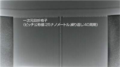
A one-dimensional grating (1D grating) is one of the most important reference standards to calibrate nanometrological instruments, such as a critical dimension scanning electron microscope. Recently, the resolutions of nanometrological instruments have become higher, and 1D grating standards with smaller pitches are required. Based on this demand, 1D gratings with 25 nm pitch consisting of Si/SiO2 multilayer thin-film structures have been developed. Furthermore, pitch calibrations using metrological atomic force microscopes (metrological AFMs) and an x-ray diffractometer have been applied. In this study, the results of a 25 nm pitch comparison between a length-and-angle-standards-traceable x-ray diffractometer and a metrological AFM are reported.
Link |
Expansion of pitch calibration range of one dimensional grating standard (AIST TODAY 2011.07)
 |
One-dimensional (1D) gratings are one of the most important transfer standards for nanometrological instruments.
Link |
Bilateral comparison of 25 nm pitch nanometric lateral scales for metrological scanning probe microscopes (Measurement Science and Technology)
|
One-dimensional (1D) and two-dimensional (2D) gratings are some of the most important transfer standards for the calibration of nanometrological instruments. National Metrology Institutes (NMIs) demonstrate their calibration capability through international comparisons among themselves and provide pitch calibration services for their customers. In the past, international comparisons were performed three times for gratings with large pitches such as 4000 nm, 1000 nm, 700 nm and 300 nm. Additionally, a bilateral comparison was conducted for 100 nm and 50 nm between the Japanese National Metrology Institute (NMIJ) and the German National Metrology Institute (PTB). The industry, however, requires calibration services for increasingly smaller pitches. In a previous study, NMIJ developed a nanometric lateral scale, a special 1D grating with 25 nm pitch consisting of Si/SiO2 multilayer thin-film structures, and calibrated the pitch of this scale by using the NMIJ's atomic force microscope equipped with differential laser interferometers (DLI-AFM). In this paper, we will report results of an informal bilateral comparison for the nanometric lateral scale between NMIJ and PTB.
Link |
Nanometric lateral scale development with Si/SiO2 multilayer thin-film structures and improvement of uncertainty evaluation using analysis of variance (Measurement Science and Technology)
|
A nanometric lateral scale (design pitch: 25 nm) with Si/SiO2 multilayer thin-film structures was developed. The pitch of the developed nanometric lateral scale was calibrated using an atomic force microscope with a differential laser interferometer, and the uncertainty in pitch measurement was evaluated. In the uncertainty evaluation, two evaluation methods were revised to avoid overestimation. The analysis of variance was applied to the evaluation of uncertainties caused by the nonuniformity of the scale and the repeatability of the measurements in the same location. The expanded uncertainties (k = 2) were 29–154 pm in this study and became smaller than 0.43 nm, which is the expanded uncertainty evaluated in our previous study.
Link |
Application of a GaAs/InGaP superlattice in nanometric lateral scales (Measurement Science and Technology)
|
The National Institute of Advanced Industrial Science and Technology (AIST), National Metrology Institute of Japan (NMIJ) developed nanometric lateral scales (design pitch: 25 nm) consisting of a GaAs/InGaP superlattice (multilayer) for atomic force microscope (AFM) and scanning electron microscope (SEM) calibration. The pitch of the fabricated nanometric lateral scales was measured using our AFM with a differential laser interferometer (DLI-AFM) and the uncertainty in the pitch measurements was evaluated. The average pitch and its expanded uncertainty (k = 2) were 25.39 nm and 0.43 nm, respectively. The quality of the developed scales was high enough to make them a suitable candidate for CRMs. On the basis of the obtained results in this technical study, the fabrication procedure and layout of the nanometric lateral scales will be optimized for the future distribution of these scales.
Link |
Ultraprecision ruler in nanometer world (AIST TODAY 2007.05)
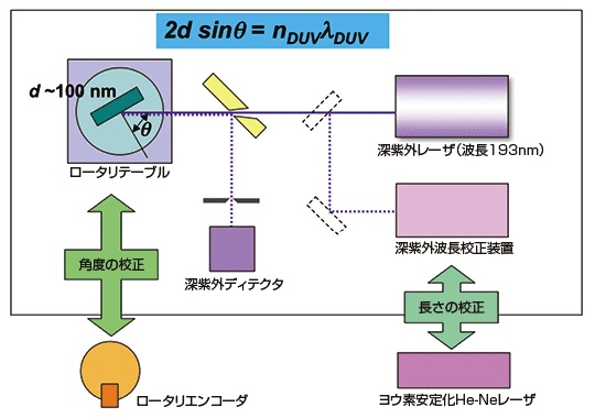 |
An ultraprecision pitch calibration system with a deep ultraviolet (DUV) laser diffractometer for rulers with the pitch of down to 97 nm has been newly constructed in collaboration with Japan Quality Assurance Organization (JQA).
Link |
Round-robin measurements of 100- and 60-nm scales among a deep-ultraviolet laser diffractometer, a scanning electron microscope and various atomic force microscopes (Measurement Science and Technology)
|
An intercomparison of nanometric lateral scales, which are special one-dimensional (1D) grating standards with sub-hundred-nanometre pitches, among a deep-ultraviolet (DUV) laser diffractometer, a critical dimension scanning electron microscope (CD-SEM) and different types of atomic force microscope (AFM) was performed. The reference value and its expanded uncertainty were provided by the National Metrology Institute of Japan (NMIJ) using an atomic force microscope with differential laser interferometers (DLI-AFM). The consistency of the measurement results obtained using the DUV laser diffractometer, CD-SEM and some AFMs was satisfactory; however, that in the measurement results obtained using other AFMs was unsatisfactory. An improvement in AFM calibration technology using nanometrological standards is required for both AFM manufacturers and AFM users, including metrology institutes.
Link |
Global standardization of scanning probe microscopy (Nanotechnology)
|
Recent efforts to achieve global standardization of scanning probe microscopy (SPM) including noncontact atomic force microscopy (NC-AFM), especially through the International Organization for Standardization (ISO) and related research, are surveyed. Since the unification of terminology for SPM is a prerequisite for standardization, it should have the first priority, followed by the unification of data management and treatment, which will enable access to and processing of SPM data collected by different types of instrument. Among the various SPM analytical methods, the dimensional metrology of SPM is regarded to be the first priority for standardization. This requires solving two basic problems: calibrating the x, y, and z coordinate axes with traceability to the SI unit of length, and eliminating the morphological artefacts caused by the shape of the probe tip. Pre-standardization efforts on restoring distorted images and characterizing the tip shape during use are discussed.
Link |
Tip characterizer for atomic force microscopy (Review of Scientific Instruments)
|
A tip characterizer for atomic force microscopy (AFM) was developed based on the fabrication of multilayer thin films. Comb-shaped line and space (LS) and wedge-shaped knife-edge structures were fabricated on a GaAs substrate. GaAs∕InGaP superlattices were used to control the width of the structures precisely, and selective chemical etching was used to form sharp edges on the nanostructures. The minimum size of the LS structure was designed to be 10nm, and the radius of the knife edge was less than 5nm. These nanostructures were used as a well-defined tip characterizer to measure the shape of a tip on a cantilever from line profiles of AFM images.
Link |
Nanometric lateral scale development using an atomic force microscope with directly traceable laser interferometers (Measurement Science and Technology)
|
One-dimensional grating standards with sub-hundred nanometre pitches are required for calibration of nanometrological instruments. Nanometric lateral scales (design pitches: 100, 60 and 50 nm) for the calibration of nanometrological instruments were designed and fabricated by electron beam cell projection lithography. An offset-locked laser system consisting of an I2-stabilized He–Ne laser and a slave laser was installed in an atomic force microscope with differential laser interferometers (DLI-AFM) for the realization of a continuously, directly length-standard-traceable system and the pitches of the lateral scales were calibrated using the new DLI-AFM. The average pitches were quite close to the design pitches and the expanded uncertainties (k = 2) were less than 0.6% of the design pitches. The developed nanometric lateral scales are of sufficiently high quality and are candidates for certified reference materials (CRMs).
Link |
Nonlinear and hysteretic influence of piezoelectric actuators in AFMs on lateral dimension measurement (Sensors and Actuators A: Physical)
|
A real-time measuring ‘Nano-metrological Atomic Force Microscope’ system equipped with an ultra-high resolution three-axis laser interferometer system is developed, in which the undesirable properties of piezoelectric actuators are compensated completely. Using this AFM and a one-dimensional (1D) grating reference standard with pitches of 240 nm, which is one of the widely used reference standards as nano-metrological lateral scales, the influences of nonlinear and hysteretic characteristics of piezoelectric actuators on image reconstruction and lateral dimension measurement are examined and compared quantitatively among three different measurement methods. The three measurement methods are: (1) the relative movement between probe tip and sample is controlled and measured directly by voltage signals applied on the XYZ scanner, the nonlinear and hysteretic characteristics of piezoelectric actuators are not compensated; (2) the relative movement between probe tip and sample is controlled by voltage signals applied on the XYZ scanner, but it is measured accurately by interferometers; (3) the relative movement between probe tip and sample in lateral directions are both controlled and measured accurately by interferometers. According to the comparison results, an accurate displacement control system is key to reduce the influences of undesirable properties of piezoelectric actuators and the developed AFM system with three-axis laser interferometer system is proved to eliminate the nonlinear and hysteretic characteristics of piezoelectric actuators completely.
Link |
Reliability of parameters of associated base straight line in step height samples: Uncertainty evaluation in step height measurements using nanometrological AFM (Precision Engineering)
|
Step height is widely used as one of the important nanometrological standards for the calibration of nanometrological instruments. In the calculation of step height, a method of determining a base straight line as a reference line is very important. In nanometrology, which is a field of dimensional metrology, an associated feature (Gaussian associated feature), such as a base straight line, is normally calculated from a measured dataset of a metrological instrument on a real feature using the least squares method. The reliability of a base straight line varies depending on the position and number of measured points for the line and the uncertainty in step height calibration also varies depending on the reliability of the base straight line. In this study, we carried the out step height measurement of micropatterned thin films (10, 7, 5, and 3 nm) using an atomic force microscope (AFM) equipped with a three-axis laser interferometer (nanometrological AFM) and evaluated the uncertainty in these measurements. From the uncertainty evaluation results, the uncertainty derived from the reliability of the parameters of the base straight line was one of the major sources of uncertainty when the measured points for the base straight line were varied. An expanded uncertainty (k = 2) of less than 0.4 nm was obtained. Furthermore, the reliable range of an associated base straight line in a single step height, such as that in an atomic step sample, was calculated and in importance of the calculation of the reliable range was shown in the uncertainty evaluation and in determining the measurement strategy.
Link |
Sub-hundred nanometre pitch measurements using an AFM with differential laser interferometers for designing usable lateral scales (Measurement Science and Technology)
|
We have developed a new atomic force microscope with differential laser interferometers (DLI-AFM), carried out test measurements of the prototype 1D-grating standards with pitches of 100, 80, 60 and 50 nm using the DLI-AFM and evaluated the uncertainty in the pitch measurements. In the procedures of the pitch calculation, two types of definitions of the peak positions, 'the centre of gravity method', and 'the zero-crossing method', were compared. The zero-crossing method was adopted in this study since the standard deviation of pitches by the zero-crossing method was smaller than that by the centre of gravity method. The expanded uncertainty (k = 2) was approximately 0.20 nm and was only 0.4% for the nominal pitch of 50 nm. We propose a design of usable 1D-grating standards as certified reference materials.
Link |
Submicrometre-pitch intercomparison between optical diffraction, scanning electron microscope and atomic force microscope (Measurement Science and Technology)
|
Intercomparison of pitch measurements for one-dimensional-grating standards (240 nm pitch), one of the widely used reference standards for nanometric lateral scales, was performed by three different methods, optical diffraction, critical dimension scanning electron microscopy and nanometrological atomic force microscopy. Average pitch values obtained by the three methods deviated by a maximum of only 0.67 nm with expanded uncertainties (k = 2) of less than 1.2 nm. The calculated En number, the index of measurement quality, of less than 1 indicates consistency of the measured pitch values and subsequent uncertainty analyses performed by three methods.
Link |
Uncertainty in pitch measurements of one-dimensional grating standards using a nanometrological atomic force microscope (Measurement Science and Technology)
|
Precision measurements of 240 nm-pitch one-dimensional grating standards were carried out using an atomic force microscope (AFM) with a high-resolution three-axis laser interferometer (nanometrological AFM). Laser sources of the three-axis laser interferometer in the nanometrological AFM were calibrated with an I2-stabilized He–Ne laser at a wavelength of 633 nm. The results of the precision measurements using the nanometrological AFM have direct traceability to the length standard. The uncertainty in the pitch measurements was estimated in accordance with the Guide to the Expression of Uncertainty in Measurement. The primary source of uncertainty in the measurements was derived from interferometer nonlinearity, and its value was approximately 0.115 nm. Expanded uncertainty (k = 2) of less than 0.31 nm was obtained. It is suggested that the nanometrological AFM is a useful instrument for the nanometrological standard calibration.
Link |