


News & Information
Qufab foundry operations for FY2026 have started. Click here for details on the application procedure. if you are interested in using our services, please feel free to contact us.
- Qufab is AIST's cleanroom facility for the fabrication of superconducting devices.
- Qufab plans to run both the PHTP and 1KP processes six times each during FY2026.
Eligible users for FY2026
For research purposes only (Domestic and international organizations, public institutions, and private companies)Deadline (1st run)
Deadline for application: Tue. March 31th, 2026Deadline for design data: Mon. April 27th, 2026 (PHSTP, 1KP)
Price
Please contact us for information on pricing.Specifications
| PHSTP Process |
4-Nb layers Nb/Al-AlOx/Nb Josephson junction layer Mo resistor layer Planarized SiO2 interlayer dielectric Minimum line width is 1.0 µm Minimum Josephson junction (JJ) is 1.0 µm square Critical current density of JJ (Jc) is 10 kA/cm2 Sheet resistance is 2.4 Ω Chip size: 7.1 x 7.1 mm 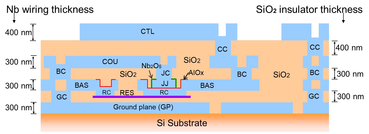 S. Nagasawa et al., IEICE Trans. Electron., vol. E104-C, no.9, pp. 435–445, Sep. 2021. |
|---|---|
| 1KP Process |
4-Nb layers Nb/Al-AlOx/Nb Josephson junction layer Pd resistor layer Planarized SiO2 interlayer dielectric Minimum line width is 1.0 µm Minimum Josephson junction (JJ) is 1.0 µm square Critical current density of JJ (Jc) is 1 kA/cm2 Sheet resistance is 1.2 Ω Chip size: 5.0 x 5.0 mm 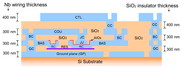 T. Yamae et al., Sci. Rep., vol. 15, 41429, 2025.. |