


News & Information
Qufab started reqruitment for the first foundry service in 2025 fiscal year in which multiple users share one wafer. Click here for details on the procedure.
Eligible users for FY2025
For research purposes only (Domestic and international organizations, public institutions, and private companies)Deadline
Deadline for application: Mon. July 14th, 2025Deadline for design data: Wed. Aug. 6th, 2025 (PHSTP), Wed. July 30th, 2025 (HSTPA)
Price
Please contact us for information on pricing.Specifications
| PHSTP Process |
4-Nb layers
Nb/Al-AlOx/Nb Josephson junction layer
Mo resistor layer
Planarized SiO2 interlayer dielectric
Minimum line width is 1.0 µm
Minimum Josephson junction (JJ) is 1.0 µm square
Critical current density of JJ (Jc) is 10 kA/cm2
Sheet resistance is 2.4 Ω
Chip size: 5 x 5 mm
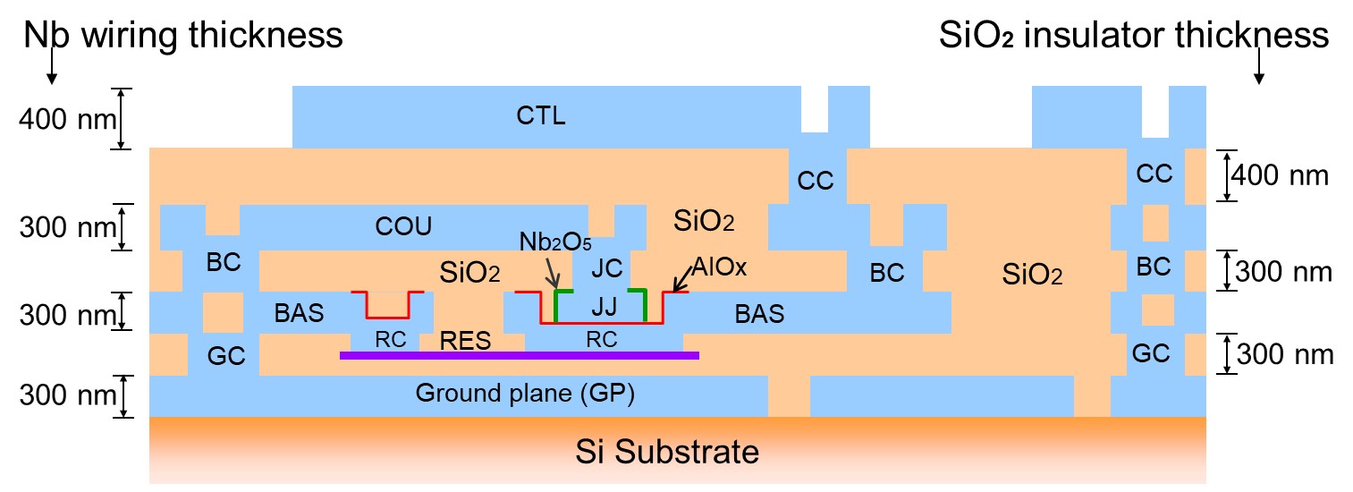 S. Nagasawa et al., IEICE Trans. Electron., vol. E104-C, no.9, pp. 435–445, Sep. 2021. |
|---|---|
| HSTP Process |
4-Nb layers
Nb/Al-AlOx/Nb Josephson junction layer
Mo resistor layer
SiO2 interlayer dielectric
Minimum line width is 1.0 µm
Minimum Josephson junction (JJ) is 1.0 µm square
Critical current density of JJ (Jc) is 10 kA/cm2
Sheet resistance is 2.4 Ω
Chip size: 7.1 x 7.1 mm
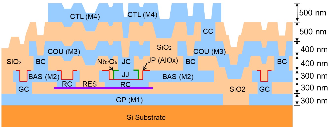 N. Takeuchi et al., Supercond. Sci. Technol., vol. 30, no. 3, Jan. 2017. |