News & Information
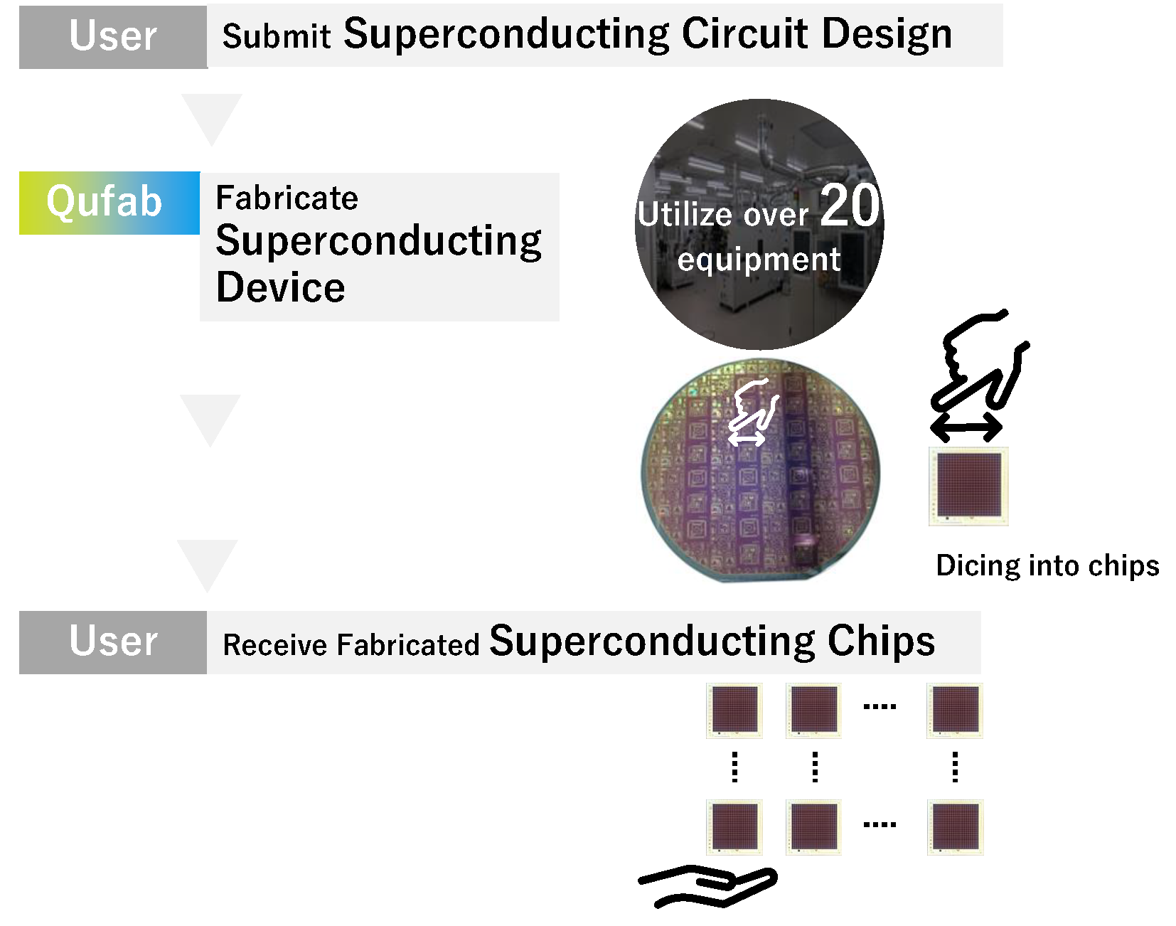
*Qufab is a cleanroom at AIST for the fabrication of superconducting devices.
| Service | We fabricate devices from your superconducting circuit design data. |
|---|---|
| On FY2024 | For research purposes only (Domestic and international organizaions, public institutions, and private companies) |
| Deadline | Deadline for application: The applications for the fiscal year 2024 have closed. Deadline for design data: Tue. Oct. 15th, 2024 (PHSTP), Wed. OcT. 2nd (HSTPA) |
| Price | Please contact us for information on pricing. |
| Procedures for the foundry |
1. User application 2. Screening by Qufab 3. Informing User with acceptance/ rejection from Qufab In the case of acceptance 4. Signing of a contract of "Technology Consulting Services*1" between AISol*2 and User 5. Advance payment of the fee from User to AISol 6. User submission of design data (in gds format) to Qufab by the date specified by Qufab 7. Device prototyping at Qufab and provision of devices with data sheet to User 8. Confirmation of Prototype data by User *1 Qufab foundry is taken place using AISol Technology Consulting Services in this year. *2 AISol(AIST Solutions Co.):The wholly owned subsidiary of AIST founded on April 1st, 2023 for the purpose to lead the national innovation ecosystem. AISol takes the lead in the contracting process and proceeds with this project as the AIST group. |
| PHSTP process |
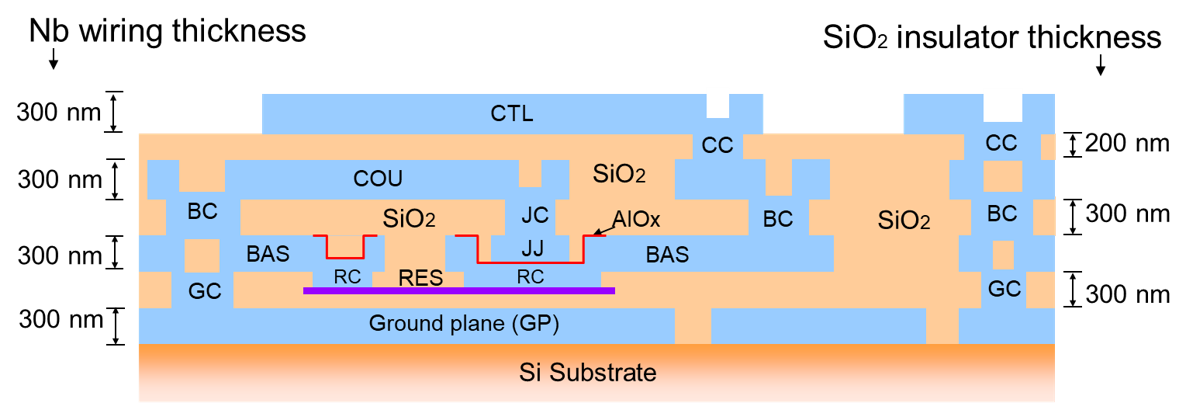
4-Nb layers Nb/Al-AlOx/Nb Josephson junction layer Mo resistor layer Planarized SiO2 interlayer dielectric Minimum line width is 1.0 μm Minimum Josephson junction (JJ) is 1.0 μm square Critical current density of JJ (Jc) is 10 kA/cm Sheet resistance is 2.4 Ω  S. Nagasawa et al., IEICE Trans. Electron., vol. E104-C, no.9, pp. 435–445, Sep. 2021. |
Contact for application and questions | M-Qufab-foundry-ml*aist.go.jp (Please convert "*" to "@".) |


