Honda R&D-AIST Diamond×Electronics Cooperative Research Laboratory
About Research
Contents
① Power semiconductor devices
【Background】 While expectations are high for the potential of diamond power devices, challenges in their actual integration into automotive inverters remain unclear due to the immaturity of the technology stage. Development has not yet reached a stage where the substrate, device, and assembly layers collaborate to accelerate progress.【Initiatives】 Develop diamond MOSFETs and automotive inverters to clarify challenges at each layer—unforeseeable through material property evaluation alone—and outline prospects for power applications.Establish and operate a diamond semiconductor hub by enhancing and expanding existing research facilities at advanced power electronics centers.
②Next-generation electronic devices
【Background】 While diamond semiconductors hold great promise as next-generation electronic devices leveraging uniquecharacteristics not foundinothersemiconductors-expanding into new application areas beyond power electronics, including high-frequency and quantum fields-development has not accelerated due to uncertainties surrounding challenges. 【Initiatives】 We will conductexploratory research on high-frequency communication devices and novel quantum devices, developing technologies to clarify the prospects for diamond semiconductor applications that contribute to the society Honda envisions.
Background and Necessity
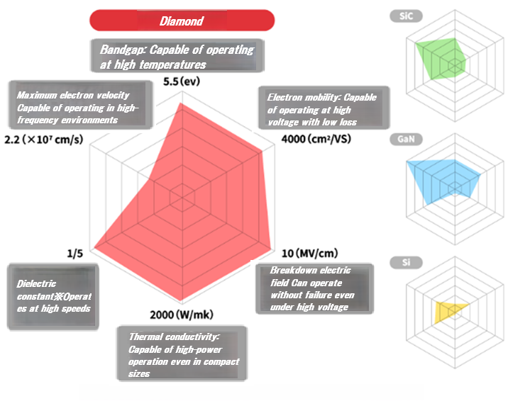
Honda's Focus on the Potential of Diamond Semiconductors
Technical Explanation
「Representative Termination Structures on Diamond Surfaces」
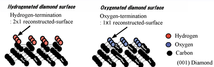
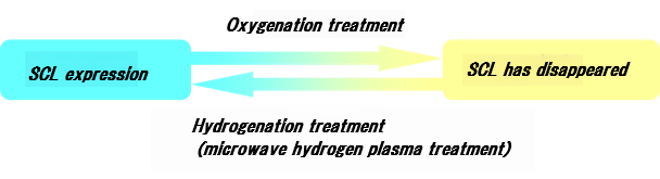
「Hydrogen-terminated surface conductive layer (SCL)」
・The surface immediately after synthesis is hydrogen-terminated and exhibits a surface conduction layer (SCL).・The SCL is a p-type semiconductor layer.
・It is characterized by high sheet carrier (hole) density and extremely low temperature dependence.
・Its origin is explained by two models: ① the transferred doping model (surface adsorbate) and ② the acceptor model.
Ref.)
・K. Hayashi et al., Appl. Phys. Lett., 68, 376 (1996).
・F. Maier et al., Phys. Rev. Lett., 85, 16, 3472 (2000).
バナースペース
Honda R&D-AIST Diamond×Electronics Cooperative Research Laboratory
(AIST Tsukuba)
AIST Tsukuba Central 2,1-1-1 Umezono, Tsukuba, Ibaraki 305-8568, Japan Telephone +81-29-861-5022
(AIST Kansai )
AIST Kansai,1-8-31,Midorigaoka,Ikeda,Osaka 563-8577, Japan Telephone +81-72-751-9601