Thin-Film Energy Device Research Group
Our research focuses on materials, devices and systems for the conversion and utilization of electrical, mechanical, optical and chemical energy, with the aim of maximizing the effective use of energy resources and further improving energy efficiency.
Research and Development Activities
Development of Manufacturing, Processing,
and Evaluation Technologies for High-Temperature Superconducting Wires
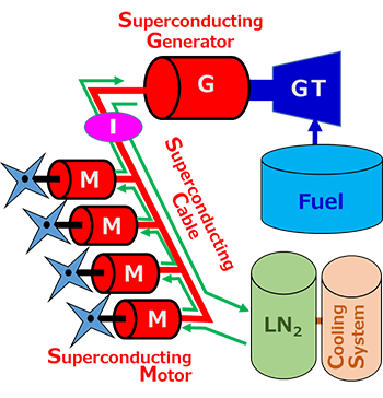
We are developing high performance RE-based superconducting wires that exhibit excellent superconducting properties even in liquid nitrogen. Specifically, we are working on material development using equipment (click to view photos)capable of handling wire lengths of several hundred meters, including process control technologies to improve critical current under magnetic fields, scribing techniques effective in reducing AC losses, and associated evaluation techniques. We are also developing various application technologies using these superconducting wires. In particular, we are developing electric propulsion systems for aircraft that use superconductivity to achieve compact, lightweight, high-efficiency and low-emission operation. As part of this effort, we are working with universities and companies to prototype and evaluate a 500 kW class fully superconducting motor and a 1 MW superconducting propulsion system, incorporating enabling technologies and achievements from wire development. This project is targeting propulsion systems for 100-200 passenger aircraft, with the aim of developing superconducting electric propulsion systems that achieve both high power density and high efficiency.
Research and Development of Novel Chalcogenide Materials
for Practical Energy Device Applications
and Abundant Material Cu2ZnSnS4 (CZTS) Solar Cells
We are researching new chalcogenide compounds, including CZTS-based compounds, and developing energy devices such as solar cells using these materials. We are also developing evaluation techniques and deposition technologies for various materials and devices, including semiconductors.
Development of Broadband Transparent Electrodes
and Enhancement of Photoelectric Conversion Device Performance
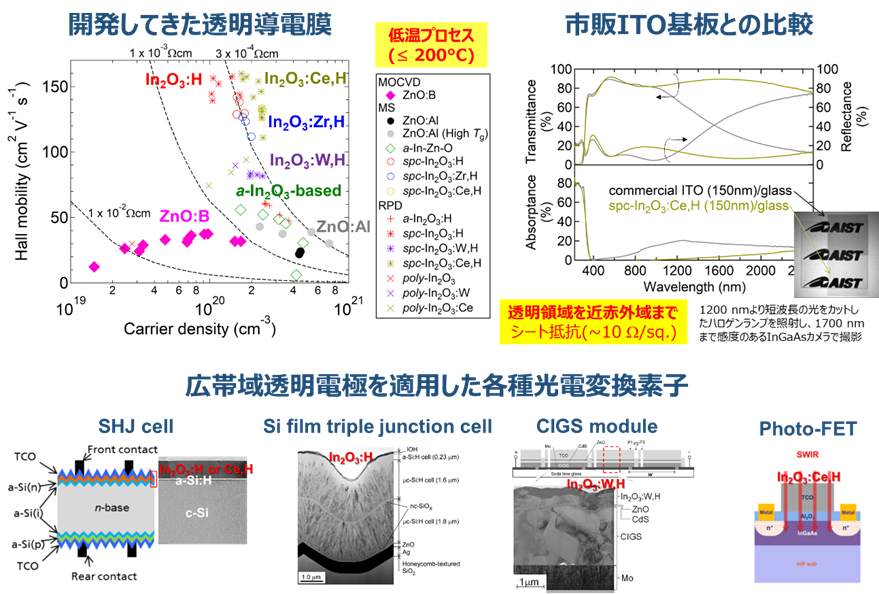
We are developing broadband transparent conductive films with high transparency from visible to near-infrared wavelengths to improve the performance of optoelectronic devices. With a focus on practical device applications, we are approaching this from both material design and low temperature, large area manufacturing processes. Polycrystalline thin films formed by low temperature processes exhibit significantly variable electronic transport properties depending on the manufacturing conditions. We are therefore comparing these films with epitaxial films grown at high temperatures to accurately understand the inherent potential of the material. One of the materials developed is In2O3:H and In2O3:TM,H (TM: transition metal, H: hydrogen) polycrystalline thin films, which exhibit exceptionally high electron mobility even when processed at temperatures below 200°C. These films are applied to silicon heterojunction solar cells and contribute to improved device performance. At the same time, the rapid expansion of solar cell production has highlighted the scarcity of indium resources. To address this, we are focusing on developing low-temperature manufacturing technology for amorphous SnO2 transparent conductive films that do not use indium. The effectiveness of these transparent conductive films is being demonstrated in collaboration with researchers inside and outside AIST by fabricating and evaluating various optoelectronic devices such as solar cells.
Notice
Members
| Positoin / Name | Area of Expertise | Location of Office |
|---|---|---|
|
Group Leader
Takashi KOIDA
|
Oxide electronics, Solar cells | Central 2 |
|
Senior Researcher
Hitoshi TAMPO
|
Semiconductor engineering, Crystal growth | Central 2 |
|
Senior Researcher
Takehiko NAGAI
|
Semiconductor engineering, surface and interface characterization, laser spectroscopy | Central 2 |
|
Specific Technical Senior Officer
Yoshiyasu SAITO
|
Electrochemistry, Lithium-ion batteries, Thermal measurement and analysis, Safety and reliability assessment | Central 2 |
|
Invited Senior Researcher
Norio TERADA
|
Solar cells, Superconductivity, Surface and interface, Photoelectron spectroscopy | Central 2 |
|
Invited Senior Researcher
Hajime SHIBATA
|
Optical material physics, Semiconductor engineering, Device physics | Central 2 |
|
Senior Researcher
Teruo IZUMI
|
Material science, Thermodynamics, Superconducting engineering | East |
|
Invited Senior Researcher
Takato MACHI
|
Superconducting wire processing technology, Solid state physics | East |
|
Postdoctoral Researcher
Hishiro HIROSE
|
Condensed matter physics, Precision measurement | East |
|
Invited Senior Researcher
Akira IBI
|
Thin film processing, Superconducting engineering | East |
|
Invited Senior Researcher
Koichi NAKAOKA
|
Materials engineering, Superconducting engineering | East |
Access
| Location | Adress | Access |
|---|---|---|
|
Central 2
|
AIST Tsukuba Central 2
1-1-1 Umezono, Tsukuba, Ibaraki 305-8568 Japan
|
AIST Tsukuba Central 2 |
|
East
|
AIST Tsukuba East
1-2-1 Namiki, Tsukuba, Ibaraki 305-8564 Japan
|
AIST Tsukuba East |
Inquiries
Please send an email to the address below.
M-tfedrg_inquire-ml@aist.go.jp