

�X�s���@�\�ޗ��`�[��(Spin Functional Materials Team)
1. �����o�[
�����`�[���� Team Leader |
Jansen Ronald | Researcher ID | Google Scholar |
|---|---|---|---|

��C������ Senior Research Scientist |
�K�� �� IBA Satoshi |
Researcher ID | |

��C������ Research Scientist |
Aurelie Spiesser | Researcher ID | |
������ Researcher |
�V�� �G�a�i�����j SAITO Hidekazu(Adjunct) |
Researcher ID | |
| ���ٌ����� Invited Senior Researcher |
��� �T�O OHNO Yuzo |
�@
2. ��Ȍ����e�[�}
| �X�s���@�\�ޗ��`�[���ł́A�s�������L���@�\�Əȓd�͐��\�����킹���X�s���g�����W�X�^��~�Ό��o�͂��\�ȃX�s�����[�U�̊�ՋZ�p�̊J���𐄐i���Ă��܂��B |
�@�X�s���g�����W�X�^
|
�d�q�̃X�s���@�\�𗘗p���������@�\��L����u�X�s���g�����W�X�^�v�̎�����ڎw����������/�����̕����X�s���f�o�C�X�̌������s���Ă��܂��B�}�Ɏ����ʂ�A�X�s���g�����W�X�^�̓\�[�X�ƃh���C���d�ɂɃX�s���̌��ƂȂ鋭�����̂��p�����邱�Ƃ��傫�ȓ����ł��B����ɂ��ASi�`���l���w�𗬂��d���͋������d�ɂ̎����������L�������X�s���ɓd���ƂȂ�A������������@�\�Ƃ��ė��p���邱�Ƃ��ł��܂��B���p�I�ȃX�s���g�����W�X�^���������邽�߂ɂ́A�X�s���ɓd�����������d�ɂ�Si�̐ڍ��E�ʂ�����ہi�X�s�������E���o�j��Si�`���l�����𗬂�Ă���ԁi�X�s���A���j�ɁA���̃X�s��������邱�Ƃ̂Ȃ����i�ʂ̐ڍ��E�ʂ�`���l���w�J�����|�C���g�ƂȂ�܂��B��X�̃O���[�v�ł́A�������d�ɂɍ��i��Fe/MgO�g���l���ڍ���p���邱�Ƃɂ��A�قڊ��S�ɃX�s���ɂ����d����Si�`���l���֒������邱�Ƃɐ��E�ŏ��߂Đ������Ă��܂��B
|
�y��v�_���z
- “Analysis of surface acoustic wave induced spin resonance of a spin accumulation”, R Jansen, P Dhagat, A Spiesser, H Saito, S Yuasa,, Physical Review B 101 (21), 214438 (2020).
- “Proximity exchange coupling in a Fe/MgO/Si tunnel contact detected by the inverted Hanle effect”, R Jansen, A Spiesser, H Saito, Y Fujita, S Yamada, K Hamaya, S Yuasa, Physical Review B 100 (17), 174432 (2019).
- “Tunnel spin polarization of Fe/MgO/Si contacts reaching 90% with increasing MgO thickness”, A Spiesser, H Saito, S Yuasa, R Jansen, Physical Review B 99 (22), 224427 (2019).
- “Hanle spin precession in a two-terminal lateral spin valve”, A Spiesser, Y Fujita, H Saito, S Yamada, K Hamaya, S Yuasa, R Jansen, Applied Physics Letters 114 (24), 242401 (2019).
- “Quantification of Spin Drift in Devices with a Heavily Doped Channel”, A Spiesser, Y Fujita, H Saito, S Yamada, K Hamaya, W Mizubayashi, Physical Review Applied 11 (4), 044020 (2019).
- “Giant spin accumulation in silicon nonlocal spin-transport devices”, A Spiesser, H Saito, Y Fujita, S Yamada, K Hamaya, S Yuasa, R Jansen, Physical Review Applied 8 (6), 064023 (2017).
- “Suppression of spin transport in ferromagnet/oxide/semiconductor junctions by magnetic impurities in the tunnel barrier”, A Spiesser, H Saito, S Yuasa, R Jansen, Applied Physics Express 9 (10), 103001 (2016).
- “Nonlinear spin transport in a rectifying ferromagnet/semiconductor Schottky contact”, R Jansen, A Spiesser, H Saito, S Yuasa, Physical Review B 92 (7), 075304 (2015).
- “Large spin accumulation voltages in epitaxial M n 5 G e 3 contacts on Ge without an oxide tunnel barrier”, A Spiesser, H Saito, R Jansen, S Yuasa, K Ando, Physical Review B 90 (20), 205213 (2014).
- “Injection and detection of spin in a semiconductor by tunneling via interface states”, R. Jansen, A. M. Deac, H. Saito, S. Yuasa, Physical Review B 85, 134420 (2012).
- “Thermal spin current and magnetothermopower by Seebeck spin tunneling”, R. Jansen, A. M. Deac, H. Saito, S. Yuasa, Physical Review B 85, 094401 (2012).
- “Thermal spin current from a ferromagnet to silicon by Seebeck spin tunneling”, Jean-Christophe Le Breton, Sandeep Sharma, Hidekazu Saito, Shinji Yuasa, Ron Jansen, Nature 475 (7354) 82-85 (2011).
- “Silicon spintronics”, Ron Jansen, Nature Materials 11 (5), 400-408 (2012).
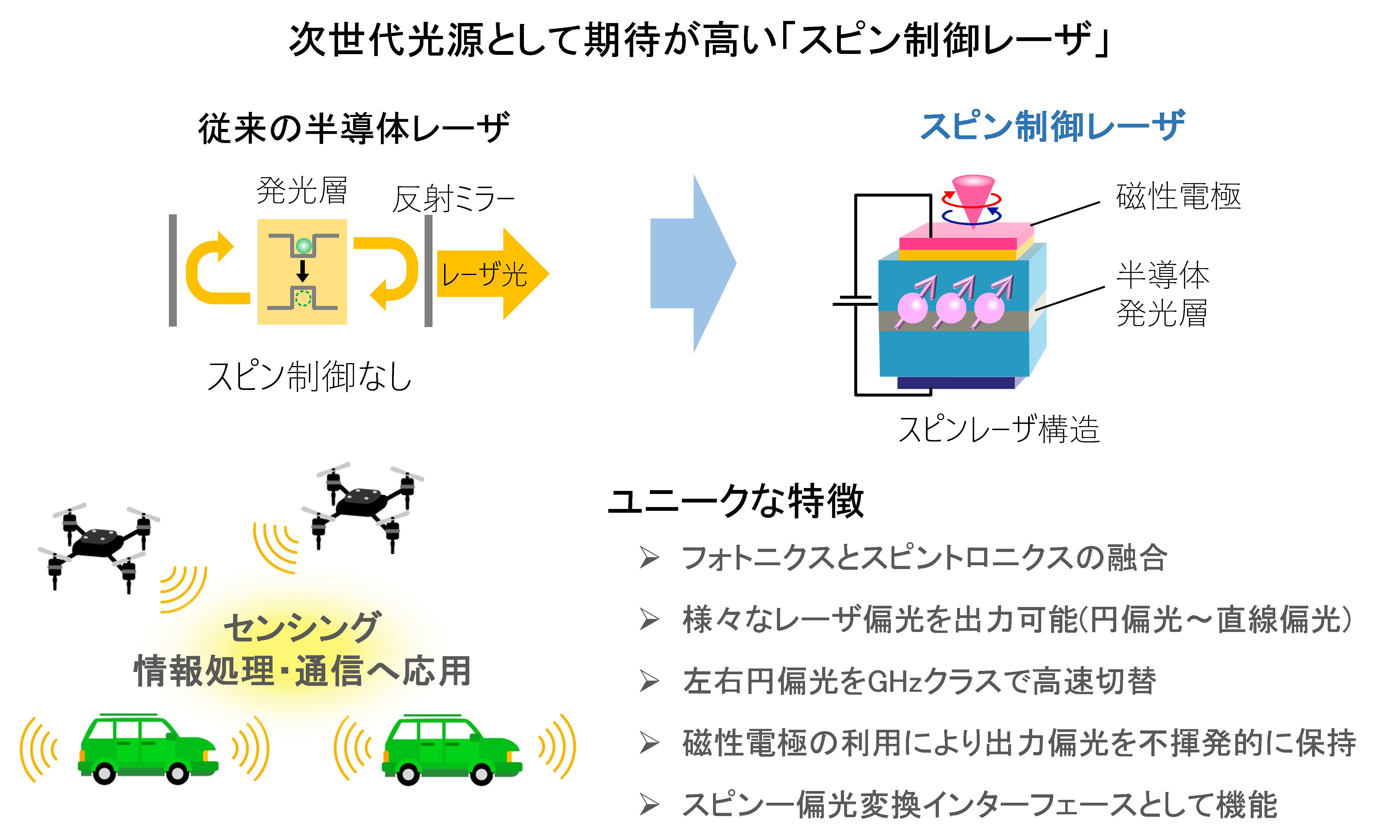
�A �X�s�����[�U
|
�d�q�̃X�s���@�\�𗘗p�����V���������̃��[�U�u�X�s�����[�U�v�̊J���𐄐i���Ă��܂��B�X�s�����[�U�͉~�Ό����璼���Ό��܂ŗl�X�ȃ��[�U�Ό����o�͂��A���A�����ȉ~�Ό��ؑ�(~GHz)���\�Ƃ���Ȃǃ��j�[�N�ȓ�����L���邱�Ƃ��玟��������Ƃ��Ē��ڂ���Ă��܂��B�X�s�����[�U���������邽�߂ɂ͎�ɂR�̗v�f�Z�p���m�����邱�Ƃ����߂��Ă��܂��B �P�j�X�s�������F�����d�ɂ�p���ăX�s���̌������������d�q���̂ɒ��� �Q�j�X�s���A���F�X�s���̌������ێ������܂ܓd�q���w�܂ŗA�� �R�j�X�s���ϊ��F�����w�ɂ����ăX�s���������̕Ό��ɍ������ɕϊ� ��X�̃`�[���ł͂����̋Z�p�ۑ�̉����Ɏ��g�݁A�i�m�b��̒����X�s��������L����X�s���A���w�┭���w�̊J���ɐ�������ȂǁA�X�s�����[�U���������[�h���鐬�ʂ��グ�Ă��܂��B
|
�y��v�_���z
- “Room temperature spin relaxation in (110)-oriented GaAs/AlGaAs superlattice with tunnel-coupled quantum wells”, Y. Ohno, S. Iba, R. Okamoto, Y. Obata, K. Obu, J. Domingez, H. Saito, Appl. Phys. Express in press.
- “Systematic study of surface morphology, photoluminescence efficiency, and spin-detection sensitivity in (110)-oriented GaAs/AlGaAs quantum wells”, S. Iba, H. Saito, K. Watanabe, Y. Ohno, S. Yuasa, Jpn. J. Appl. Phys. 55, 113001 (2016).
- “Growth condition dependence of photoluminescence polarization in (100) GaAs/AlGaAs quantum wells at room temperature”, S. Iba, H. Saito, K. Watanabe, Y. Ohno, S. Yuasa, J. Appl. Phys. 118, 083901 (2015).
- “Fabrication of Ge-based light-emitting diodes with a ferromagnetic metal/insulator tunnel contact”, S. Iba, H. Saito, S. Yuasa, Y. Yasutake, S. Fukatsu, Jpn. J. Appl. Phys. 54, 04DM02 (2015).
- “Reducing Schottky barrier height for Fe/n-GaAs junction by inserting thin GaOx layer”, H Saito, Y Mineno, S Yuasa, K Ando, J. Appl. Phys. 109, 07C701 (2011).
- “Efficient spin injection into semiconductor from an Fe/GaOx tunnel injector”, H. Saito, J.C. Le Breton, V. Zayets, Y. Mineno, S. Yuasa, K. Ando, Appl. Phys. Lett. 96, 012501 (2010).
- “Highly Enhanced Electron-Injection Efficiency in GaAs-Based Light-Emitting Diodes Using a Fe/GaOx Tunnel Injector”, H. Saito, J.C. Le Breton, V. Zayets, S. Yuasa, K. Ando, Appl. Phys. Express 2, 083003 (2009).
- “Low effective barrier height of GaOx tunnel barrier in metal/semiconductor hybrid junctions”, J.C. Le Breton, H. Saito, S. Yuasa, K. Ando, Appl. Phys. Lett. 94, 152101 (2009).
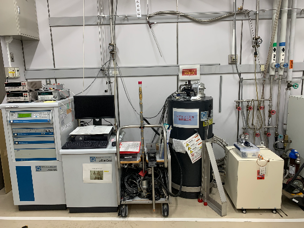
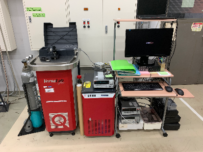
3. ��Ȍ����ݔ��E�Z�p�̏Љ�
| (1) �������u 3��̕��q���G�s�^�L�V�[���u����g���Ĕ�����/�≏��/�����������琬��n�C�u���b�h�\����[�U�ELED�\���̍��i���Ȑ����Z�p��L���Ă��܂��B |
|
| (2) �����E�ቷ�d�C���葕�u 2���PPMS(�����������葕�u)�𗘗p���ėl�X�ȉ��x�E���E���ɂ����ēd�C������s�����Ƃ��\�ł��B |
|
| (3) ���w�����]�����u �p���X(�s�R�b)����јA���g�̔g���ό���(700~1000nm)�┒�F�n���Q�������v���𗘗p���Ď����̌��w����(����/�z��/����)���L�ш�(300~2000nm)�ŕ]�����邱�Ƃ��\�ł��B |
4. ��ȊO�������v���W�F�N�g�A�O���A�g
|
�i�s���̊O�������v���W�F�N�g
�E�O���A�g�F
|
5. �ߋ��̎�ȃv���X���\�ւ̃����N
2016�N 2012�N 2011�N |