

�s�����������`�[�� (Non-Volatile Memory Team)
1. �����o�[
 �@
�@�����`�[���� Team Leader |
��� ���s NOZAKI Takayuki |
Researcher ID | Google Scholar |
|---|---|---|---|

��C������ Senior Research Scientist |
�b�쓡 �^ KONOTO Makoto |
Researcher ID | |

��C������ Research Scientist |
�R�{ ���� YAMAMOTO Tatsuya |
Researcher ID | |
������ Research Scientist |
���� �� SUGIHARA Atsushi |
Researcher ID | |

������ Research Scientist |
��m�� �q�_ IHINOSE Tomohiro |
Researcher ID | |
 �@
�@�����`�[���t Research Scientist |
��� �F�� NOZAKI Tomohiro |
Researcher ID | |
���ٌ����� Invited Senior Researcher |
��� �`�� SUZUKI Yoshishige |
Researcher ID | Google Scholar |
2. ��Ȍ����e�[�}
|
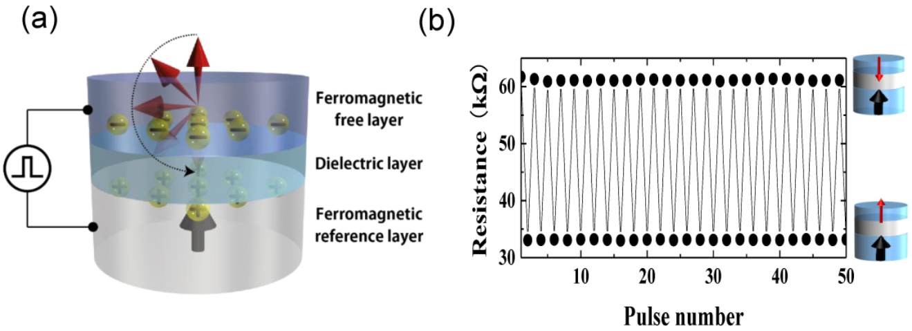
�s�����������`�[���ł͓d������^MRAM(VC-MRAM: Voltage-controlled Magnetoresistive Random Access Memory)�̊�Ռ����J���Ɏ��g��ł��܂��BMRAM�͎��������̎���(�X�s��)�̌����Ƃ��ĕs�����ɏ���ۑ����邱�Ƃ��ł��邽�߁A�ҋ@�d�̓[���̃��[�L���O���������������҂���Ă��܂��B���������ݐ��i�J������MRAM�ł͓d���ɂ����̏������݂��s���Ă��邽�߁ASRAM��DRAM�ȂNJ����̊������������Ɣ�r���ċ쓮�d�͂����ɑ傫���_���ۑ�ƂȂ��Ă��܂��B�����ʼn�X�͓d���ɂ��V�����X�s������Z�p���J�A�ҋ@�d�͂����łȂ��쓮�d�͂����������ɂ̕s�������������AVC-MRAM����邱�ƂŁAIoT�G�b�W�f�o�C�X��o�C��AI�R���s���[�e�B���O�Ȃǂ̋ߖ���IT�@��̒����d�͉��Ɋ�^���邱�Ƃ�ڎw���Ă��܂��B��̓I�Ȍ����e�[�}�Ƃ��ẮA�@�d������^�g���l�����C��R�f�q�p�̐V�K�ޗ��T���A�A�d���������]�Z�p�̊J���A����чB�d���U�N�X�s�����ۂ̕����𖾂ȂǂɎ��g��ł��܂��B �i�Q�l�_���j T. Nozaki (Q-4838-2017) et al. "Recent progress in the voltage-controlled magnetic anisotropy effect and the challenges faced in developing voltage-torque MRAM(Review)", micromachines 10, 327 (2019). |
�@ �d������^�g���l�����C��R�f�q�p�̐V�K�ޗ��T��
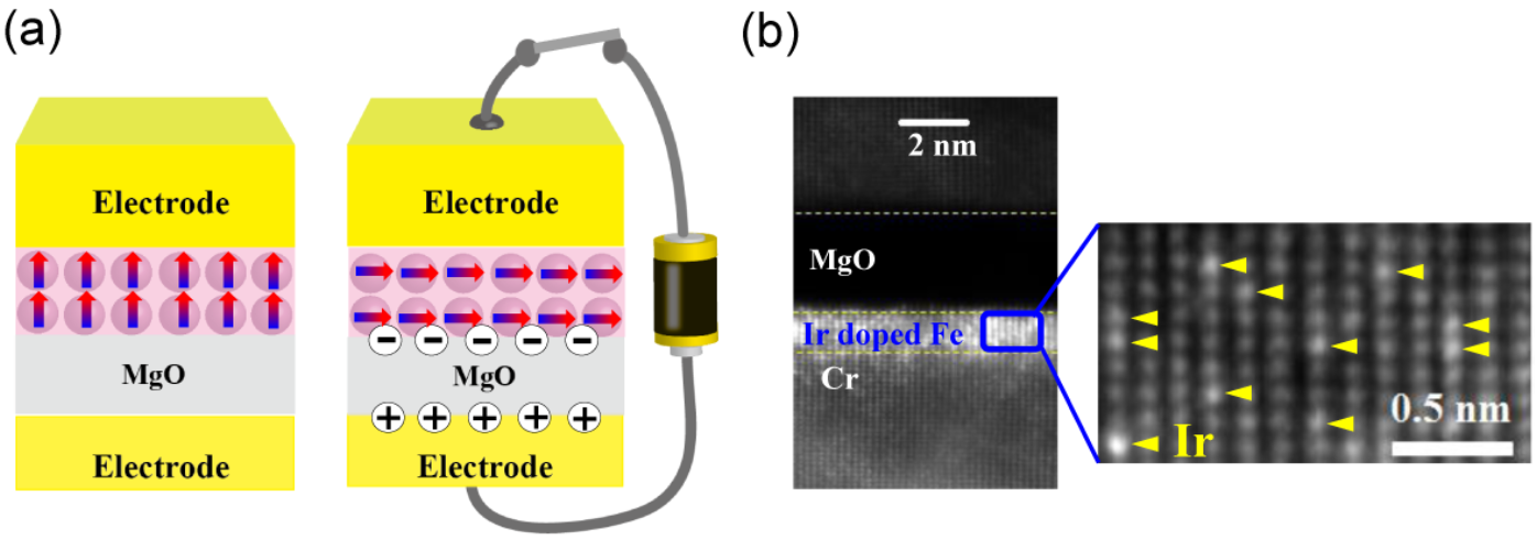
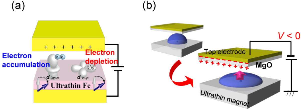
| �@�d������^�g���l�����C��R�f�q�ł́A�d�����C�ٕ�������(VCMA: Voltage-controlled magnetic anisotropy)�ƌĂ�錻�ۂ𗘗p���ēd���ɂ��X�s���̌����𐧌䂵�܂��B���C�ٕ����Ƃ̓X�s���̌����₷�����������肷�镨���l�ł���A�ʏ�͕����ŗL�̒l�ł����A�����q�w���x���ɒ������������������w(FeCo�����Ȃ�)��p����Ɠd���ɂ�萧�䂷�邱�Ƃ��\�ƂȂ�܂��BVCMA���ʂ�p�����d������^MRAM���������邽�߂ɂ͏����ȓd���ő傫�����C�ٕ������ω����钴�����������w�A�g���l����Ǒw�Ȃǂ̐V�ޗ���T�����邱�Ƃ��d�v�ƂȂ�܂��B���O���[�v�ł͂���܂łɃC���W�E�����Z�x�Ńh�[�s���O�����������S�Ȃǂɂ����āA��������\��VCMA���ʂƂ��Ă͐��E�ō����\��B�����Ă��܂�(�}1)�B |
�A �d���������]�Z�p�̊J��
| �@VCMA���ʂ𗘗p�����������]�A�܂���̏������݂ɂ͍����p���X�d������ɂ�鎥���̍��^���𗘗p���܂�(�}2)�B���̓d���U�N�_�C�i�~�b�N�������]�́A��fJ/bit�̏������݃G�l���M�[��1�i�m�b�I�[�_�[�̍����������݂��\�Ƃ��܂��B���̋Z�p�͈���̋ɐ��̃p���X�d���ŏ������݂��\(���j�|�[��)�Ȃ��߁A��H�̊ȑf����ǂݏo�����̌돑�����݂����Ȃ��_�����_�ƂȂ�܂����A����ŏ������݃G���[�̒ጸ��bit�ԃo�����̗}�����ۑ�ƂȂ��Ă��܂��B�ޗ������̌���ɉ����āAVCMA���ʂ𗘗p�����X�s���_�C�i�~�N�X�̐��䓙�𗘗p���Ă��̉��P��}���Ă��܂��B |
�B�d���U�N�X�s�����ۂ̕�����
| �@�d���ɂ��X�s������̌��������コ���邽�߂ɂ͂��̕����N���̗������d�v�ƂȂ�܂��B����܂ő���w�Ⓦ�k��w�𒆐S�Ƃ����O���@�ւƂ̘A�g�ɂ��VCMA���ʂ̋N���𖾂Ɏ��g�݁A�d������ɂ���Ē����������w/�U�d�w�E�ʂɗU�N���ꂽ�~�ϓd�ׂɂ��d�q��L���ω���d�E�ɂ��d�q���z�̕ω����d�v�ł��邱�Ƃ𖾂炩�ɂ��Ă��܂���(�}3)�B�����̒m�����ޗ��v�Ƀt�B�[�h�o�b�N���A����Ȃ���������ڎw���Ă��܂��B���̑��A�V���������N���ɂ��d���X�s������Z�p�̊J��AMRAM�ȊO�̓d������^�X�s���g���j�N�X�f�o�C�X�ւ̓W�J�ɂ����g��ł��܂��B |
3. ��Ȍ����ݔ��E�Z�p�̏Љ�
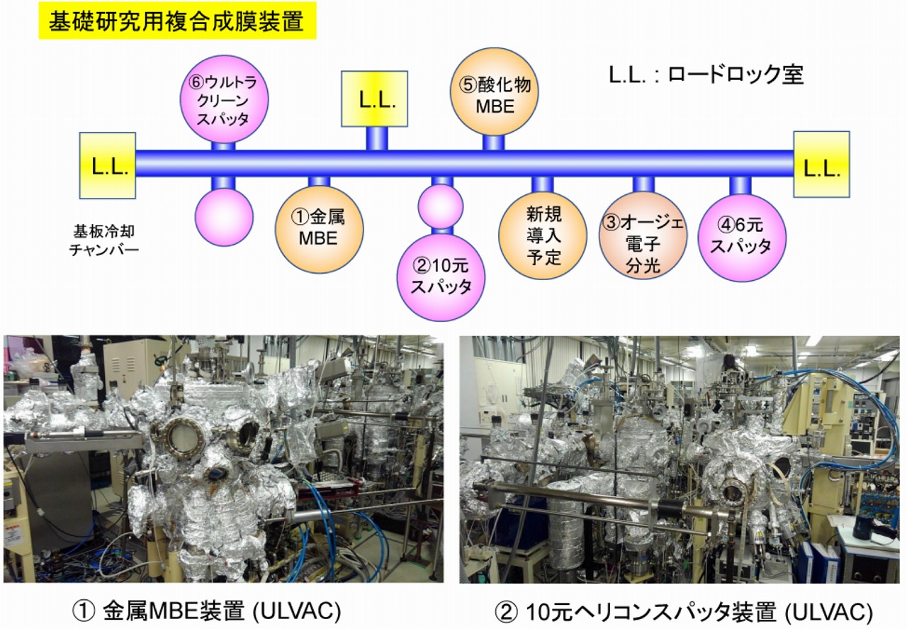
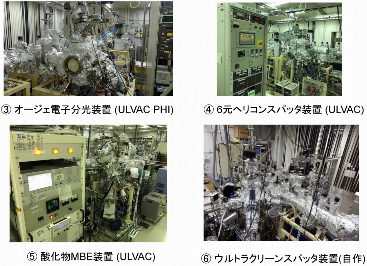
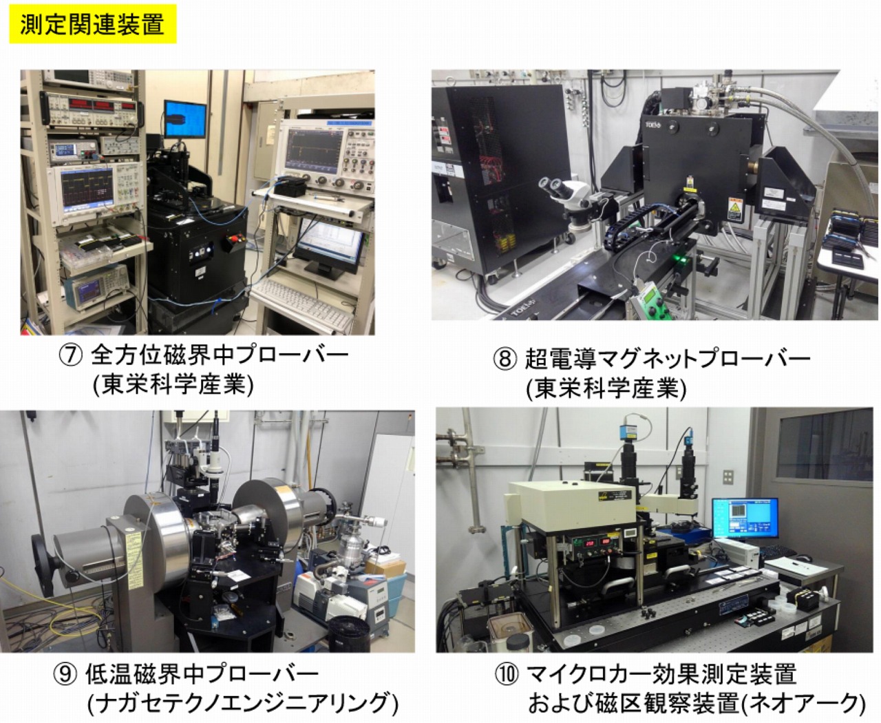
[��b�����p�����������u]�@�����^��������ŕ����̐������u��ڑ�����2�C���`�E�F�[�n�Ή������������u�ł��BMBE3��(��1���2020�N�x���ɐV�K�X�V�\��)�A�}�O�l�g�����X�p�b�^���u3��A�\�ʕ��͑��u1��ƃ��[�h���b�N��3���L���Ă��܂��B�g�ݍ��킹�ɂ����60��ދ߂��ޗ����C�\�I���邱�ƂȂ����w�ϑw�����邱�Ƃ��\�ł��B [����֘A���u]�@���E������ɂ����鎥�����w���̎��C��R�����]�����s����X�̎��E���v���[�o�[�A�v���[�o�[�Ή��^�}�C�N���J�[���ʑ��u�A����ώ@���u�A�ቷ���E���v���[�o�[�A����э����g�֘A���葕�u�Q��L���Ă��܂��B |
4. ��ȊO�������v���W�F�N�g�A�O���A�g
�@|
�@�u�������E�����������\�Ƃ���AI�`�b�v�E������R���s���[�e�B���O�̋Z�p�J��/������R���s���[�e�B���O�Z�p�̊J��/�d���쓮�s��������������p�������ȓd�̓u���C�������t�B�b�N�V�X�e���̌����J���v �A�u�|�X�g5G���ʐM�V�X�e����Ջ��������J������/�����J�����ڇ@ �|�X�g5G���ʐM�V�X�e���̊J��/�|�X�g5G���ʐM�V�X�e���̂��߂̊v�V�I�s����������������ь��`���Z�p�̌����J���v |
5. �ߋ��̎�ȃv���X���\�ւ̃����N
�@|
�@���q�w����ɂ�莥�C�������[�f�q�̕��R������ю��C���萫�����P �A�������ȓd���X�s��������������鎥�C�������[�p�ޗ����J���@2017.12.01�f�� �B�d���������ݕ������C�������[�̏������݃G���[�������I�ɒጸ�@2017.07.12�f�� �C���q�̌`��ς��Ē��ȃG�l���M�[���C�������@2017.06.26�f�� �D�s���������C�������̂��߂̐V���ȓd���쓮�������ݕ������J���@2016.12.05�f�� �E�d���������ݕ����s�������������[�̈��蓮��̎��Ə������݃G���[���]�� |
6. ��Ș_�����X�g
�@2020
|