Tandem Photovoltaic Research Team
Toward the Creation of Novel Silicon-based Solar Cell Devices
Overview
Photovoltaic power generation is expected to play a central role in realizing a carbon-neutral society.
Crystalline silicon solar cells, which currently account for more than 95% of the global market, require new technologies that lead to high efficiency and low cost, tandem solar cells that exceed the efficiency limits of silicon, sustainable manufacturing technologies to further expand their use, and the development of innovative devices for emerging applications.
Research Target
- Simultaneous realization of higher performance and reduction in cost of crystalline silicon solar cells through advancements in new material and process technologies.
- Development of tandem solar cell technology to achieve efficiencies exceeding 30% and methods to support their industrial-scale production.
- Development of resource-efficient and sustainable manufacturing technologies for device production.
- Development of new applications and creation of new markets.
Research Outline
Research Themes
Our team is pursuing the following research themes to develop technologies that minimize the trade-off between conversion efficiency and manufacturing cost, to develop multi-junction technologies that surpass the limitations of silicon, and to create innovative devices for emerging applications.
- Development of functional materials (amorphous and nanocrystalline silicon, metal oxides, etc.) that provide surface defect passivation and selective charge carrier extraction for crystalline silicon solar cells using thin-film growth techniques such as plasma-enhanced chemical vapor deposition (PECVD) and atomic layer deposition (ALD).
- Development of perovskite/silicon tandem solar cells and associated process technologies to support their industrialization.
- Development of Si wafer cutting technology and the following edge surface passivation, and structural coloring technology for crystalline silicon solar cells, enabling their application in building facades and windows.
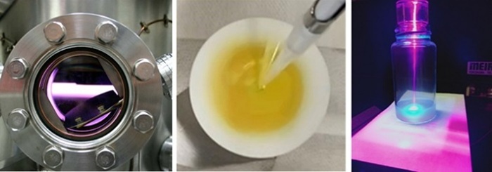
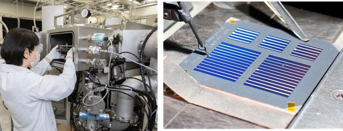
(Left: Plasma CVD, Center: Spin-coating, Right: Laser-induced nanomaterial synthesis)
Activities and Achievements
Development of ultra-thin crystalline silicon solar cells
We have been working on the development of technology to inactivate (passivate) surface defects of crystalline Si, which is important for improving the performance of crystalline silicon solar cells, by making full use of the amorphous and nanocrystalline silicon thin-film deposition technology.
As a result, we have demonstrated a conversion efficiency of 23.3% and a world-leading open-circuit voltage (754 mV) using ultra-thin crystalline silicon wafers with a thickness of ~50 μm (1/2~1/3 of the conventional thickness).
In addition, we have demonstrated that such ultra-thin solar cells lead to improved performance under high-temperature conditions.
This advancement is expected to increase actual power generation in the outdoor operation, reduce silicon consumption, and enable applications on curved surfaces such as buildings and vehicles.
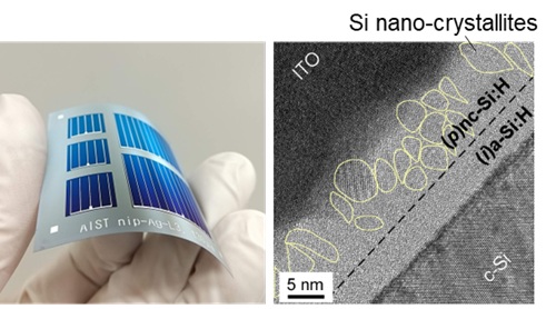
(Right) Cross-sectional transmission electron microscope image of the crystalline silicon/amorphous silicon (a-Si:H)/nanocrystalline silicon (nc-Si:H) heterojunction interface used in the device
Development of crystalline silicon solar cells using emerging technologies
We are also developing new materials to replace amorphous silicon-based thin films.
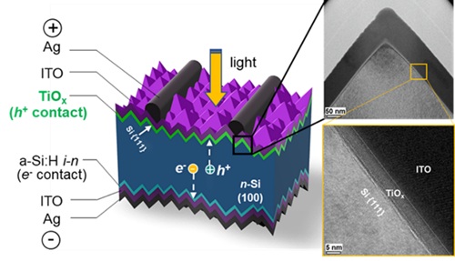
For example, titanium oxide (titanium dioxide) is known to act as an electron-selective contact for crystalline silicon.
However, with the work in collaboration with the Fraunhofer Institute for Solar Energy Systems ISE and the University of Oxford, our team has discovered a new function of surface passivation and selective extraction of positive charge (holes) from crystalline silicon by forming a thin (~5 nm) titanium oxide film on the surface of crystalline silicon, deposited using ALD.
We have demonstrated conversion efficiencies exceeding 20%, paving the way for practical applications.
In addition, we fabricated a crystalline silicon solar cell featuring both hole- and electron-selective passivating contacts composed entirely of a single material (TiOx), without the need for extrinsic doping.
Furthermore, this technology has been implemented in a novel interconnection scheme for perovskite/Si tandem solar cells (refer to the next research result).
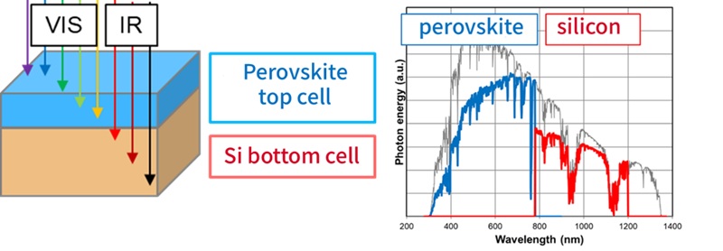
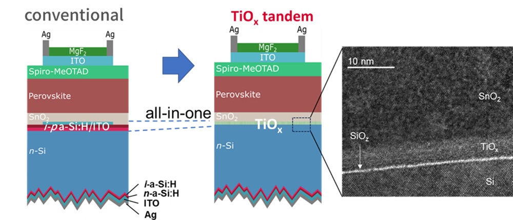
Development of perovskite/crystalline silicon tandem solar cells
The theoretical efficiency limit of crystalline silicon solar cells is approximately 29%, and higher efficiencies cannot be obtained with silicon alone.
Tandem solar cells, in which a crystalline silicon solar cell is stacked together with a perovskite solar cell, are attracting attention as a type of solar cell that can exceed the efficiency limit of silicon.
In the pursuit of higher efficiencies, there has been a tendency to increase the number of component layers, thereby increasing device complexity and processing cost.
Notably, indium-based oxides (ITO, etc.) are often used, particularly for the recombination layer (p/n reverse junction layer) that interconnects the perovskite-top cell and silicon-bottom cell, which increases the number of manufacturing steps and involves the use of scarce metals, and results in increased optical losses.
We have demonstrated that a TiOx layer (~3-5 nm) grown by atomic layer deposition (ALD) enables a series interconnection of a perovskite n-i-p top cell with a silicon wafer directly.
The TiOx layer serves as an all-in-one interconnect, fulfilling the functions of silicon surface passivation, hole extraction from silicon, and recombination junction at the top/bottom cell interface.
As a result, the developed tandem device represents as high performance as the reference tandem that uses amorphous silicon passivating selective contacts and an indium-tin-oxide interlayer.
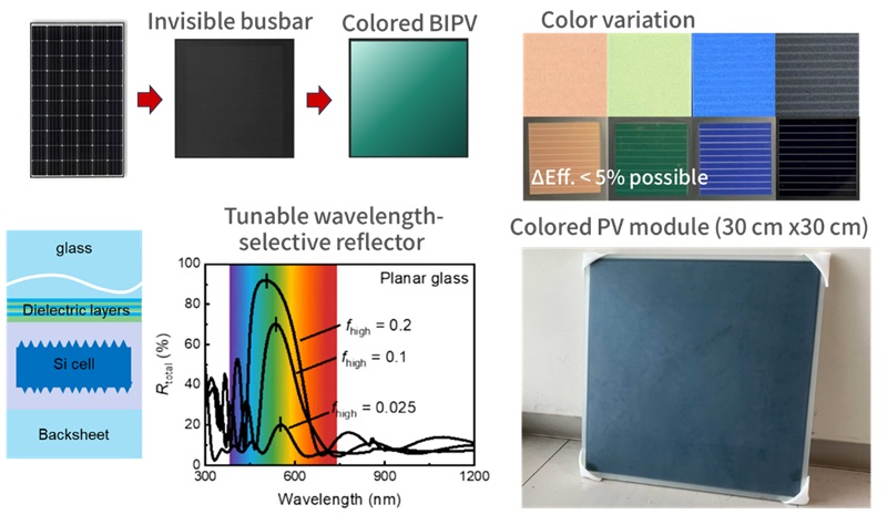
Research and development of crystalline silicon solar cells for building windows and facades
Development is expected to address location constraints and promote multi-purpose applications of solar cells, such as for lightweight roofs, automotive integration, and building-integrated materials for zero-energy buildings (ZEB).
Conventional solar cell modules are typically black in color which makes them less visually compatible with building materials.
In this research, we developed a technology for building-integrated, color-controlled photovoltaic modules that combine aesthetic excellence with high-efficiency power generation.
By controlling the structures of dielectric multilayers and textured glass surface, we successfully reduced optical losses while achieving high color tone uniformity (small angular dependence) in the colored modules.
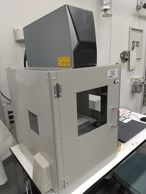
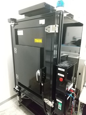
Main Research Facilities
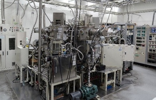
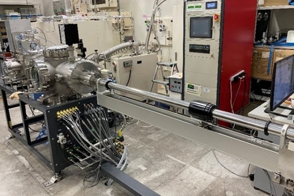
Multi-chamber plasma-enhanced chemical vapor deposition (PECVD) system
Used for growing amorphous silicon and nanocrystalline silicon thin films.
Thin-film silicon films with p- or n-type doping or without doping (i-type) can be deposited in independent chambers.
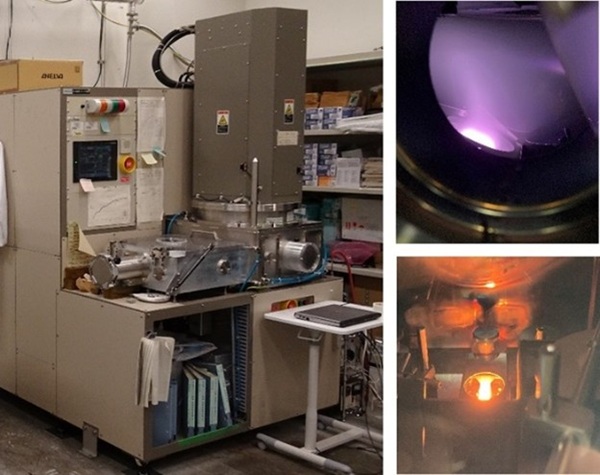
Atomic layer deposition (ALD) system
Used for the growth of metal compound thin films such as titanium oxide, titanium nitride, tin oxide, and aluminum oxide, with thicknesses of a few nanometers.
Electrode and thin-film coating systems (magnetron sputtering, thermal evaporation)
These apparatuses are used to form transparent electrodes (ITO, ZnO, etc.), metal electrodes (Al, Ag, Au), charge transport layers (C60, MoO3, etc.), and antireflection coatings for solar cells.
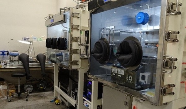
Glovebox
Perovskite solar cells can be fabricated in dry air or nitrogen atmosphere.
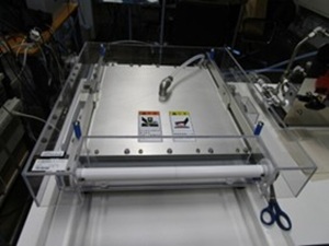
Compact laminator
Small solar cell modules can be fabricated for research and development.
Laser processing equipment
Crystalline silicon solar cells and various substrates can be cut and processed into any desired shape.
Photoluminescence measurement setup
Photoluminescence enables diagnostic imaging to access the quality of crystalline silicon wafers and solar cells at each process step.
Team Member
| Title | Name |
|---|---|
| Leader, Team | MATSUI Takuya |
| Chief Senior Researcher | SAI Hitoshi |
| Senior Researcher | SVRCEK Vladimir |
| Senior Researcher | SHOJI Yasushi |
| Researcher | IKEDA Takuto |
| Attached to Research Team | MIZUNO Hidenori |