Silicon Photonics Research Team
Group Outline and Primary Goal
Silicon photonics is a high-density photonic integration platform technology based on the fabrication technology of silicon electronic devices and circuits. This cutting-edge technology provides us ultra-compact, energy-efficient and cost-effective photonic circuits, and also has superior reliability and capability of electronic-photonic integration. Therefore, this technology can be a breakthrough to the realization of SDGs via wide applications from information systems to sensing. For the industrial development and further radicalization of this technology, in our team, following research and development are intensively performed.
1) Standard silicon photonics technology based on the state-of-art fabrication technologies and design methods.
2) Advanced silicon photonics based on heterogeneous material integration, machine learning and neural network technologies.
3) Construction of a silicon photonics R&D eco system for open innovation.
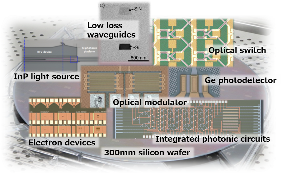
Fig. 1. Photonic integration with silicon photonics technology.
Key Themes of Research
-Standard Silicon Photonics Technology
Feature 1: Low loss and Large scale photonic integration utilizing the state-of-art fabrication technology
・Utilizing a 45-nm node silicon fabirication line: LER ≲ 1nm
・Silicon waveguide with the world's lowest propagation loss: ~1dB/cm
・World's largest scale photonic integration utilizing high-uniformity fabrication process
Feature 2: High-performance photonic devices based on sophisticated design technologies
・Simulation of optical propagation, photonic devices performance and integrated photonic circuits
・Simulation of electron device performance and CMOS fabrication process (TCAD)
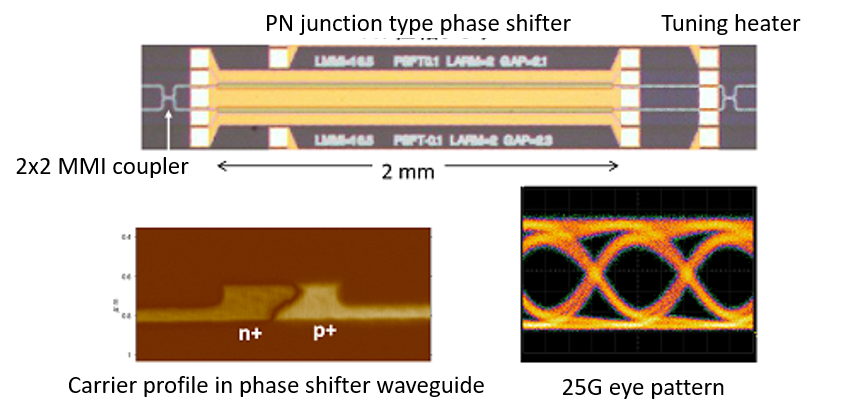
・Design and fabrication of high performance devices: low loss fiber coupling structure, high-speed optical molulator (Fig.2) etc...
Feature 3: Compilation of process design kit (PDK)
・Standardization of fabrication process and design rules
・Preparation of design check tools and device library
 -Advanced Silicon Photonics Technology
Feature 1: Multi-functinal photonic device integration with heterogeneous material integration
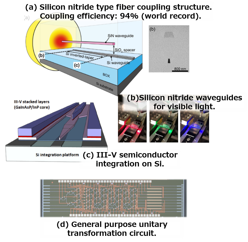
・Ultra-low loss fiber coupling structure utilizing a silicon nitride(Fig. 3(a))
・Silicon nitride based visible light waveguides for sensor applications(Fig.3(b)
・III-V semiconductor device integration utilizing a micro-transfer printing technology(Fig. 3(c))
・High efficiency optical comb generation utilizing graphene-loaded waveguides
Feature 2: Highly-functional applications of integrated photonic circuits
・Ultra-low latency neuromorphic computing utilizing unitary transformation interference circuits(Fig.3(d))
・Arbitrary function reconfiguration of integrated photonic circuits utilizing machine learning algorithms
 -Silicon Photonics Ecosystem
Feature 1: Open innovation system based on Silicon Photonics Consortium
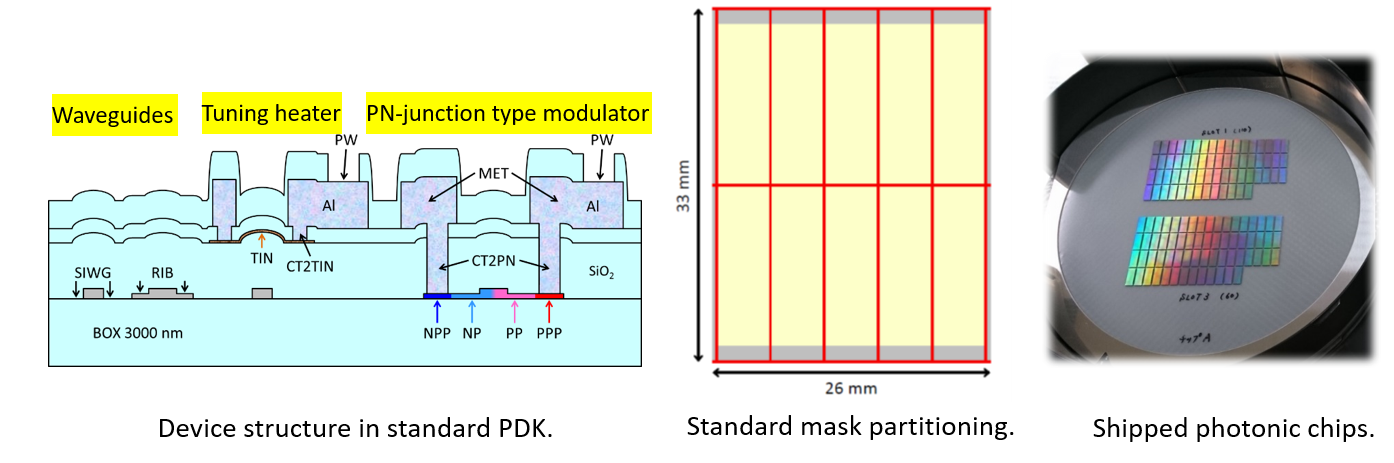
・Shuttle and dedicated fabrication service available(Fig.4)
・Development of value chain technologies: design, assembly and testing
Feature 2: Direct collaboration with AIST
・Information and communications: Photonic device integration for compact and energy efficient network systems
・Measurement technology: Optical comb generation, ultra short pulse measurement
・Sensing: LIDAR etc....
Feature 1: Low loss and Large scale photonic integration utilizing the state-of-art fabrication technology
・Utilizing a 45-nm node silicon fabirication line: LER ≲ 1nm
・Silicon waveguide with the world's lowest propagation loss: ~1dB/cm
・World's largest scale photonic integration utilizing high-uniformity fabrication process
Feature 2: High-performance photonic devices based on sophisticated design technologies
・Simulation of optical propagation, photonic devices performance and integrated photonic circuits
・Simulation of electron device performance and CMOS fabrication process (TCAD)
・Design and fabrication of high performance devices: low loss fiber coupling structure, high-speed optical molulator (Fig.2) etc...
Feature 3: Compilation of process design kit (PDK)
・Standardization of fabrication process and design rules
・Preparation of design check tools and device library
Fig.2. Silicon optical modulator.
Feature 1: Multi-functinal photonic device integration with heterogeneous material integration
・Ultra-low loss fiber coupling structure utilizing a silicon nitride(Fig. 3(a))
・Silicon nitride based visible light waveguides for sensor applications(Fig.3(b)
・III-V semiconductor device integration utilizing a micro-transfer printing technology(Fig. 3(c))
・High efficiency optical comb generation utilizing graphene-loaded waveguides
Feature 2: Highly-functional applications of integrated photonic circuits
・Ultra-low latency neuromorphic computing utilizing unitary transformation interference circuits(Fig.3(d))
・Arbitrary function reconfiguration of integrated photonic circuits utilizing machine learning algorithms
Fig.3. Selected results of advanced silicon photonics research.
Feature 1: Open innovation system based on Silicon Photonics Consortium
・Shuttle and dedicated fabrication service available(Fig.4)
・Development of value chain technologies: design, assembly and testing
Feature 2: Direct collaboration with AIST
・Information and communications: Photonic device integration for compact and energy efficient network systems
・Measurement technology: Optical comb generation, ultra short pulse measurement
・Sensing: LIDAR etc....
Fig.4. Introduction of AIST silicon photonics shuttle service.
Our Technologies
- Photonic device design and measurement
- Photonics-electronics integration design
- Si photonics fabrication process design
- Silicon nitride waveguide fabrication
- Heterogeneous material integration
Articles
- Y. Maegami, M. Okano, G. Cong, K. Suzuki, M. Ohno, T. Narushima, N. Yokoyama, M. Seki, M. Ohtsuka, S. Namiki, and K. Yamada, “Simple and fully CMOS-compatible low-loss fiber coupling structure for a silicon photonics platform," Optics Letters, 45, pp. 2095-2098 (2020).
https://doi.org/10.1364/OL.388267 - K. Suzuki, R. Konoike, N. Yokoyama, M. Seki, M. Ohtsuka, S. Saitoh, S. Suda, H. Matsuura, K. Yamada, S. Namiki, H. Kawashima, K. Ikeda, “Nonduplicate Polarization-Diversity 32x32 Silicon Photonics Switch Based on a SiN/Si Double-Layer Platform,” J. Lightwave Technol., vol.38-2,pp.226-232 (2020).
https://doi.org/10.1109/JLT.2019.2934763 - K. Suzuki R. Konoike, S. Suda, H. Matsuura, S. Namiki, H. Kawashima, K. Ikeda, “Low-loss Low-Crosstalk, and Large-Scale Optical Switch Based on Silicon Photonics,” J. Lightwave Technol., vol.38-2,pp.233-239、(2020).
https://doi.org/10.1109/JLT.2019.2934768 - R. Kou, Y. Kobayashi, S. Inoue, T. Tsuchizawa, Yuko Ueno, S. Suzuki, H. Hibino, T. Yamamoto, H. Nakajima, and K. Yamada, “Dopamine detection on activated reaction field consisting of graphene-integrated silicon photonic cavity," Opt. Express,27-22,pp.32058-32068 (2019).
https://doi.org/10.1364/OE.27.032058 - R. Kou, N. Yamamoto, G. Fujii, T. Aihara, T. Tsuchizawa, A. Ishizawa, K. Hitachi, H. Gotoh, M. Ukibe, and K. Yamada, “Spectrometric analysis of silicon nitride films deposited by low-temperature liquid-source CVD," J. APPLIED PHYSICS,126-13,pp.133101 (2019).
https://doi.org/10.1063/1.5114675 - G. Cong, N. Yamamoto, T. Inoue, M. Okano, Y. Maegami, M. Ohno and K. Yamada, “Arbitrary reconfiguration of universal silicon photonic circuits by bacteria foraging algorithm to achieve reconfigurable photonic digital-to-analog conversion,” Opt. Express, vol. 27(18), pp.24914-24922 (2019).
https://doi.org/10.1364/OE.27.024914 - G. Cong, M. Okano, Y. Maegami, M. Ohno and K. Yamada, “Interferometric autocorrelation of ultrafast optical pulses in silicon sub-micrometer p-i-n waveguides,” Opt. Express, vol. 26(12), pp.15090-15100 (2018).
https://doi.org/10.1364/OE.26.015090 - G. Cong, M. Ohno, Y. Maegami, M. Okano, and K. Yamada, “Silicon traveling-wave Mach–Zehnder modulator under distributed-bias driving,” Optics Letters, Vol. 43 No. 3, pp.403-406 (2018).
https://doi.org/10.1364/OL.43.000403 - Y. Maegami, G. Cong, M. Ohno, M. Okano, K. Itoh, N. Nishiyama, S. Araim and K. Yamada, “High-efficiency strip-loaded waveguide based silicon Mach-Zehnder modulator with vertical p-n junction phase shifter,” Opt. Express, Vol. 25 No. 25, pp.31407-31416 (2017).
https://doi.org/10.1364/OE.25.031407 - C. Cong, M. Ohno, Y. Maegami, M. Okano, and K. Yamada, “Optical autocorrelation performance of silicon wire p-i-n waveguides utilizing the enhanced two-photon absorption,” Opt. Express, Vol. 24 No. 26, pp.29452-29458 (2016).
https://doi.org/10.1364/OE.24.029452 - Y. Maegami, G Cong, M. Ohno, M. Okano, and K. Yamada, “Strip-loaded waveguide-based optical phase shifter for high-efficiency silicon optical modulators,” Photonics Research, Vol. 4 No. 6, pp. 222-226 (2016).
https://doi.org/10.1364/PRJ.4.000222 - Y. Maegami, R. Takei, C. Cong, M. Ohno, M. Okano, T. Horikawa, K. Yamada and T. Kamei, “Hydrogenated amorphous silicon waveguide with vertical pin structure for infrared detection,” Electronics Letters, Vol. 53 No.20 pp.1705-1707 (2016).
https://doi.org/10.1049/el.2016.2359 - Y. Maegami, M. Okano, G. Cong, M. Ohno, K. Yamada, “Completely CMOS compatible SiN-waveguide-based fiber coupling structure for Si wire waveguides,” Opt. Express, Vol. 24 No. 15, pp.16856-16865 (2016).
https://doi.org/10.1364/OE.24.016856 - Y. Maegami, R. Takei, E. Omoda, T. Amano, M. Okano, M. Mori, T. Kamei, and Y. Sakakibara, “Spot-size converter with a SiO2 spacer layer between tapered Si and SiON waveguides for fiber-to-chip coupling,” Opt. Express, Vol. 23 No. 16, pp.21287-21295 (2015).
https://doi.org/10.1364/OE.23.021287 - G.W. Cong, T. Matsukawa, T. Chiba, H. Tadokoro, M. Yanagihara, M. Ohno, H. Kawashima, H. Kuwatsuka, Y. Igarashi, M. Masahara, and H. Ishikawa, "Large current MOSFET on photonic silicon-oninsulator wafers and its monolithic integration with a thermo optic 2 × 2 Mach Zehnder switch", Opt. Express, Vol. 21 No. 6, pp.6889-6894 (2013).
https://doi.org/10.1364/OE.21.006889