Optics Integration Research Team
Group Outline and Primary Goal
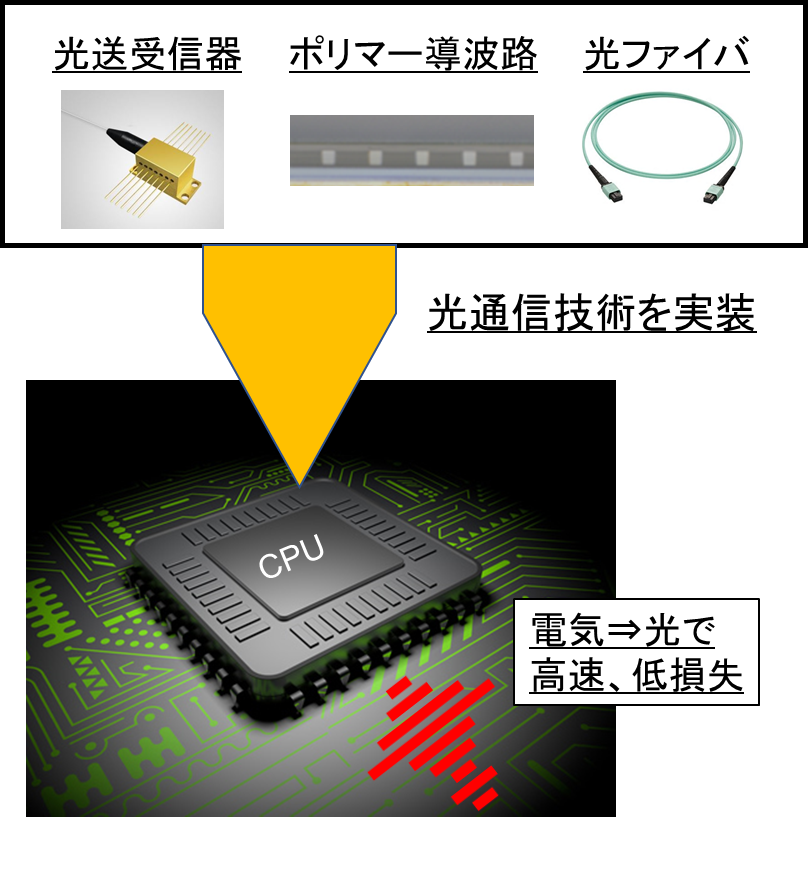
Currently, we are making advances in large-scale systems such as data centers, that are making significant improvements in our lives. However, there are limits to improving system performance by relying on miniaturization of semiconductor devices, and other methods will be needed in order to further improve performance.
Our team is conducting research and development into areas such as high-precision integration technology for connecting optical devices, and optical packaging technology for integrating optical devices into electronics devices, and we are aiming to implement opto-electronic co-packaging which will be a core technology of the combined opto-electronic computers of the future.
Furthermore, we are conducting joint research with various national projects and the private sector in order to take the developed optical integration technology to implementation in society. In particular, we are currently participating in the Photonics Electronics Technology Research Association (PETRA) in the "NEDO Development of Technologies for Super Energy-Efficient Optical Electronics Implementation Systems" and are responsible for optical integration technology.
Key Themes of Research
The optical multimode approach is suitable for practical applications because connection is relatively easy due to the large diameter of waveguide (around 50 μm). The problem is that massive parallelization is required in order to handle large capacity optical signals. We have the technology for fabricating 96 ch multimode polymer optical waveguides, mounting high-density (125 μm spacing) multicore (24 ch) optical connectors, and high-speed optical signal evaluation technology (Fig. 1).
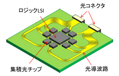
Schematic structure
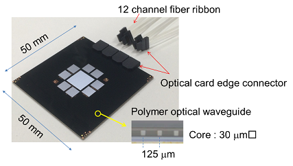
Prototype sample
Figure 1: Opto-electrical hybrid package board with integrated multimode polymer optical waveguides and multicore optical cable with optical connectors for circuit boards
(2) Opto-electronic co-packaging exceeding 10 Tbps using single modeSince wavelength multiplexing can be used with single-mode light, it is possible to handle high-speed signals in excess of 10 Tbps. However, since the waveguide diameter is only 10 μm, optical mounting is difficult. Furthermore, the optical waveguide of silicon photonics that has been attracting attention in recent years has become even smaller at less than 1 μm2, which cannot be handled by current technology. Because of this, we have been conducting research and development related to single-mode opto-electronic co-packaging which integrates each of the components from research and development to create technology for optical mountings for single-mode silicon photonic devices, and for optical packaging. More specifically, we fabricated a prototype three-dimensional mirror for silicon photonics (Fig. 2) and a prototype single-mode polymer waveguide (Fig. 3), mounted an optical connector on a single-mode polymer waveguide, and performed an evaluation of each.
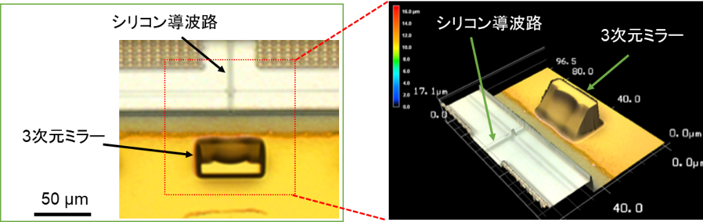
Figure 2 Three-dimensional mirror for silicon photonics
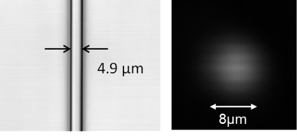
Figure 3 Single-mode polymer waveguide and corresponding single-mode beam properties
Our Technologies and Equipment
- Optical packaging
- Polymer optical waveguide fabrication and evaluation
- Optical connector design and mounting
- High-speed optical signal evaluation
Articles
- A. Noriki, I. Tamai, Y. Ibusuki, A. Ukita, S. Suda, D. Shimura, Y. Onawa, H. Yaegashi, and T. Amano, “Mirror-based silicon-photonics vertical I/O with coupling efficiency enhancement for standard single-mode fiber,” J. Lightwave Technol., 38, 3147-3155 (2020).
https://doi.org/10.1109/JLT.2020.2995915 - T.Kurosu, S.Suda, H.Matsuura, and S. Namiki, "Stable operation of silicon photonic switches in field-deployed optical path network," IEICE Electronics Express, vol.16 issue2 (2019).
https://doi.org/10.1587/elex.16.20181058 - S. Suda, H. Matsuura, K. Tanizawa, K. Suzuki, K. Ikeda, H. Kawashima, and S. Namiki, "Fast and Accurate Automatic Calibration of a 32 × 32 Silicon Photonic Strictly-Non-Blocking Switch," Proc. of Photonics in Switching 2017, PTu3C.5. (2017).
https://doi.org/10.1364/PS.2017.PTu3C.5 - T. Amano, S. Ukita, Y. Egashira, M. Sasaki, A. Noriki, M. Mori, K. Kurata, and Y. Sakakibara, “25-Gb/s Operation of a Polymer Optical Waveguide on an Electrical Hybrid LSI Package Substrate With Optical Card Edge Connector,” J. Lightwave Technol. 34, 3006-3011 (2016).
https://doi.org/10.1109/JLT.2016.2518216