Hybrid Photonics Research Team
Group Outline and Primary Goal
The hybrid photonics research team is conducting research and development aiming to build a framework for new hybrid photonics technology to enable further development of existing technology by integrating dissimilar materials and different technologies on a silicon photonics platform. We are engaged in a wide range of research activities from fundamentals to applications including dissimilar materials integration devices in which different types of materials such as compound semiconductors, Ge, etc. are integrated on a silicon photonics platform, combined silicon photonics/photonic crystal devices in which photonic crystal resonators and optical waveguides are integrated, fiber connection devices (elephant couplers) applying unique 90 degree bends in a direction perpendicular to a silicon waveguide, optical transmission devices that utilize these base technologies, optical arithmetic circuits, and LiDAR.
Key Themes of Research
Building a framework for hybrid photonics technology that integrates dissimilar materials and different technologies on a silicon photonics platform
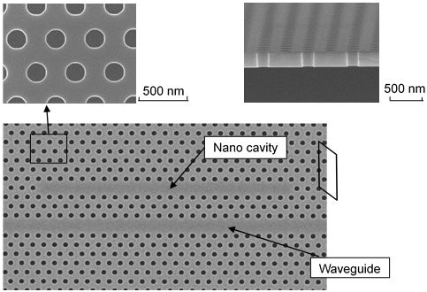
Figure 1: Photonic crystal optical resonator and optical waveguide
Press release (March 16, 2016) "Successful mass production of optical nano-resonators that have the world highest Q value" - Anticipated utilization in product manufacturing lines and research sites -
URL:
https://www.aist.go.jp/aist_j/press_release/pr2016/pr20160316/pr20160316.html
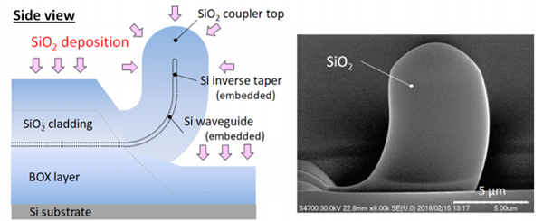
Figure 2: Fiber connection device (elephant coupler) that uses technology to machine perpendicular bends in silicon waveguides
Press release (January 28, 2016) "Development of revolutionary silicon photonics optical input/output technology" - Great advance towards integration of optics and electronics in unique surface perpendicular coupling -
URL:https://www.aist.go.jp/aist_j/new_research/2016/nr20160128/nr20160128.html
Our Technologies and Equipment
- Design and evaluation of silicon photonics platforms
- Fabrication of silicon photonics platforms using a 300 mm wafer silicon experimental production line
- Machining perpendicular bends in silicon waveguides
We are providing a silicon photonics platform for integration of dissimilar materials and different technologies as a "VICTORIES Open Innovation Hub". This will assist with the design, fabrication, and evaluation of silicon photonics platforms that use a 300 mm wafer silicon experimental production line.
Articles
- Q. Li, C.P. Ho, H. Tang, M. Okano, K. Ikeda, S. Takagi, and M. Takenaka, "Si racetrack optical modulator based on the III–V/Si hybrid MOS capacitor," Opt. Express 29, 6824-6833 (2021).
https://doi.org/10.1364/OE.418108 - T. Yasuda, M. Okano, M. Ohtsuka, M. Seki, N. Yokoyama, and Y. Takahashi, "Raman silicon laser based on a nanocavity fabricated by photolithography," OSA Continuum 3, 814-823 (2020).
https://doi.org/10.1364/OSAC.389114 - Y. Atsumi, T. Yoshida, E. Omoda, and Y. Sakakibara, "Low-Loss and Broadband Optical Coupler Based on Lensed-Top Vertically Curved Silicon Waveguide," IEEE Photon. Technol. Lett. 31, 603-606 (2019).
https://doi.org/10.1109/LPT.2019.2903233 - K. Ashida, M. Okano, T. Yasuda, M. Ohtsuka, M. Seki, N. Yokoyama, K. Koshino, K. Yamada, and Y. Takahashi, “Photonic Crystal Nanocavities With an Average Q Factor of 1.9 Million Fabricated on a 300-mm-Wide SOI Wafer Using a CMOS-Compatible Process,” J. Lightwave Technol. 36, 4774-4782 (2018).
https://doi.org/10.1109/JLT.2018.2861894 - Y. Atsumi, T. Yoshida, E. Omoda, and Y. Sakakibara, "Broad-band surface optical coupler based on a SiO2-capped vertically curved silicon waveguide," Opt. Express 26, 10400-10407 (2018).
https://doi.org/10.1364/OE.26.010400 - K. Ashida, M. Okano, M. Ohtsuka, M. Seki, N. Yokoyama, K. Koshino, M. Mori, T. Asano, S. Noda, and Y. Takahashi, "Ultrahigh-Q photonic crystal nanocavities fabricated by CMOS process technologies," Opt. Express 25, 18165-18174 (2017).
https://doi.org/10.1364/OE.25.018165 - T. Yoshida, E. Omoda, Y. Atsumi, T. Nishi, S. Tajima, N. Miura, M. Mori, and Y. Sakakibara, “Vertically Curved Si Waveguide Coupler with Low Loss and Flat Wavelength Window,” J. Lightwave Technol. 34, 1567-1571 (2016).
https://doi.org/10.1109/JLT.2015.2506732